by Dr. Jaydeep T. Vagh 😇
INTRO.
he world of electrical and electronics is quite closely related, yet sometimes far apart in terms of size and magnitude. Whereas electrical equipment could be mostly bulky electrical motors of various types, the electronic items are normally in the shorter version. In this article we will study one such aspect namely the microprocessor which, apart from several other functions, also serves as the heart of the computer on which you are probably reading this article.
forms the brain of the Central Processing Unit (CPU). Microprocessor is an engine which can compute various operations fabricated on a single chip. The internal
Evolution of Microprocessor
The first microprocessor was introduced in the year 1971. It was introduced by Intel and was named Intel 4004.
Intel 4004 is a 4 bit microprocessor and it was not a powerful microprocessor. It can perform addition and subtraction operation on 4 bits at a time.
architecture of microprocessor determines what operations can be performed on a microprocessor and how it can be performed. Let us take a look at a brief history of the microprocessor and discuss how the microprocessors have evolved over the past years.

However it was Intel’s 8080 was the first microprocessor to make it to Home computers. It was introduced during the year 1974 and it can perform 8 bit operations. Then during the year 1976, Intel introduced 8085 processors which is nothing but an update of 8080 processors.8080 processors are updated by adding two Enable/Disable Instructions, Three added interrupt pins and serial I/O pins.
Intel introduced 8086 pins during the year 1976. The major difference between 8085 and 8086 processor is that 8085 is an 8 bit processor, but 8086 processor is a 16 bit processor.
The greatest advantage of the above processors are that it do not contain Floating point instructions. Here floating point refers to the radix point or decimal point. For example: 123.456 is a floating point representation. Processors such as 8085 and 8086 do not support such representations and instructions.

Intel later introduced 8087 processor which was the first math co-processor and later the 8088 processor which was incorporated into IBM personal computers.
As the years progressed lots of processors from 8088,80286,80386,80486,Pentium II, Pentium III, Pentium IV and now Core2Duo,Dual Core and Quad core processors are the latest in the market.
Apart from Intel, there are some other manufacturers who produce the CMOS version of 8085 microprocessor. Such manufacturers are called second source manufacturers.
MOS stands for COMPLEMENTARY METAL OXIDE SEMICONDUCTOR. It is a technology used in Microprocessors and Microcontrollers for making Integrated circuits.
The devices which are made of CMOS have high immunity towards noise and the static power consumption is low.
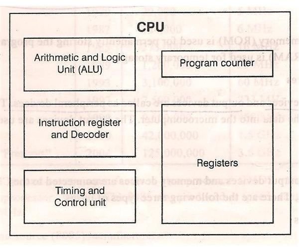
Basic Microprocessor
A basic microprocessor requires certain elements to perform some operation. To perform an operation microprocessor requires:
Registers may be called as the Internal Storage device. Input data, Output data and various other binary data is stored in this unit for further processing.
Control unit as the name specifies controls the flow of data and signals in the microprocessor. It generates the necessary control signals for various data that are fed to microprocessor.

All the instructions that are fetched from memory are located in the Instruction register. So the Instruction register is used to store various information’s that microprocessor requires in order to carry out an operation.

Program Counter (PC):
Program counter stores the address of the next instruction to be executed. It is usually denoted as PC.
Advantages of microprocessor
- High processing speed
- Compact size
- Easy maintenance
- Can perform complex mathematics
- Flexible
- Can be improved according to requirement
Disadvantages of microprocessors
- Overheating occurs due to overuse
- Performance depends on size of data
- Large board size than microcontrollers
- Most microprocessors do not support floating point operations
Evolution of Microprocessors
Transistor was invented in 1948 (23 December 1947 in Bell lab). IC was invented in 1958 (Fair Child Semiconductors) By Texas Instruments J kilby. First microprocessor was invented by INTEL(INTegrated ELectronics).
Size of microprocessor – 4 bit
| Name | Year of Invention | Clock speed | Number of transistors | Inst. per sec |
|---|---|---|---|---|
| INTEL 4004/4040 | 1971 by Ted Hoff and Stanley Mazor | 740 KHz | 2300 | 60,000 |
Size of microprocessor – 8 bit
| Name | Year of Invention | Clock speed | Number of transistors | Inst. per sec |
|---|---|---|---|---|
| 8008 | 1972 | 500 KHz | 50,000 | |
| 8080 | 1974 | 2 MHz | 60,000 | 10 times faster than 8008 |
| 8085 | 1976 (16 bit address bus) | 3 MHz | 6500 | 769230 |
Size of microprocessor – 16 bit
| Name | Year of Invention | Clock speed | Number of transistors | Inst. per sec |
|---|---|---|---|---|
| 8086 | 1978 (multiply and divide instruction, 16 bit data bus and 20 bit address bus) | 4.77 MHz, 8 MHz, 10 MHz | 29000 | 2.5 Million |
| 8088 | 1979 (cheaper version of 8086 and 8 bit external bus) | 2.5 Million | ||
| 80186/80188 | 1982 (80188 cheaper version of 80186, and addtional components like interuppt controller, clock generator, local bus controller,counters) | 6 MHz | ||
| 80286 | 1982 (data bus 16bit and address bus 24 bit) | 8 MHz | 134000 | 4 Million |
Size of microprocessor – 32 bit
| Name | Year of Invention | Clock speed | Number of transistors | Inst. per sec |
|---|---|---|---|---|
| INTEL 80386 | 1986 (other versions 80386DX, 80386SX, 80386SL and data bus 32 bit address bus 32 bit) | 16 MHz – 33 MHz | 275000 | |
| INTEL 80486 | 1986 (other versions 80486DX, 80486SX, 80486DX2, 80486DX4) | 16 MHz – 100 MHz | 1.2 Million transistors | 8 KB of cache memory |
| PENTIUM | 1993 | 66 MHz | Cache memory 8 bit for instructions 8 bit for data |
Size of microprocessor – 64 bit
| Name | Year of Invention | Clock speed | Number of transistors | Inst. per sec |
|---|---|---|---|---|
| INTEL core 2 | 2006 (other versions core2 duo, core2 quad, core2 extreme) | 1.2 GHz to 3 GHz | 291 Million transistors | 64 KB of L1 cache per core 4 MB of L2 cache |
| i3, i5, i7 | 2007, 2009, 2010 | 2.2GHz – 3.3GHz, 2.4GHz – 3.6GHz, 2.93GHz – 3.33GHz |
Generations of microprocessor:
1st Generation: This was the period during 1971 to 1973 of microprocessor’s history. In 1971, INTEL created the first microprocessor 4004 that would run at a clock speed of 108 KHz. During this period, the other microprocessors in the market including Rockwell international PPS-4, INTEL-8008 and National semiconductors IMP-16 were in use. But, all these were not TTL compatible processors.
2nd Generation: This was the period during 1973 to 1978 in which very efficient 8-bit microprocessors were implemented like Motorola 6800 and 6801, INTEL-8085 and Zilogs-Z80, which were among the most popular ones. Owing to their superfast speed, they were costly as they were based on NMOS technology fabrication.
3rd Generation: During this period 16 bit processors were created and designed using HMOS technology. From 1979 to 1980, INTEL 8086/80186/80286 and Motorola 68000 and 68010 were developed. Speeds of those processors were four times better than the 2nd generation processors. X
4th Generation: From 1981 to 1995 this generation developed 32 bit microprocessors by using HCMOS fabrication. INTEL-80386 and Motorola’s 68020/68030 were the popular processors.
5th Generation: From 1995 to until now this generation has been bringing out high-performance and high-speed processors that make use of 64-bit processors. Such processors include Pentium, Celeron, Dual and Quad core processors.
Thus, microprocessor has evolved through all these generations, and the fifth generation microprocessors represent advancement in specifications. Therefore, some of the processors from the fifth generation of processors with their specifications are briefly explained below.
🧐 Objectives 🧐
- Describe N-type and P-type semiconductors.
- Understand the operation of diodes and transistors.
- Understand the difference between different types of transistors.
- Describe Moore’s law and some of its implications.
- Be aware of limits to scaling transistors and wires in integrated circuits.
- Describe different schemes for scaling interconnects.
- Explain the difference between “lead microprocessors” and “compactions.”
- List possibilities for future transistor scaling.
Processors are the brains of computers. Other components allow a computer to store or retrieve data and to input or output data, but the processor performs computations and does something useful with the data.
It is the processor that determines what action will happen next within
the computer and directs the overall operation. Processors in early computers were created out of many separate components, but as technology improved it became possible to integrate all of the components of a processor onto a single piece, or chip, of silicon. These integrated circuits are called microprocessors. Today microprocessors are everywhere. Supercomputers are designed to perform calculations using hundreds or thousands of microprocessors. Even personal computers that have a single central processor use other processors to control the display, network communication, disk drives, and other functions. In addition, thousands of products we don’t think of as
computers make use of microprocessors. Cars, stereos, cell phones, microwaves, and washing machines all contain microprocessors. which are used as the central processing units of computers, but what makes processors so ubiquitous is their ability to provide many different functions. Some computer chips are designed to perform a single very specific function, but microprocessors are built to run programs. By designing the processor to be able to execute many different instructions in any order, the processor can be programmed to perform whatever function is needed at the moment. The possible uses of the processor are limited only by the imagination of the programmer. This flexibility is one of the keys to the microprocessor’s success. Another is the steady improvement of performance. Over the last 30 years, as manufacturing technologies have improved, the performance of microprocessors has doubled roughly every 2 years. 1 For most products, built to perform a particular function, this amount
of improvement would be unnecessary. Microwave ovens are an improvement on conventional ovens mainly because they cook food more quickly, but what if instead of heating food in a few minutes, they could be improved even more to only take a few seconds? There would probably be a demand for this, but what about further improvements so that it took only tenths of a second, or even just hundredths of a second. At some point, further improvements in performance of a single task
become meaningless because the task being performed is fast enough. However, the flexibility of processors allows them to constantly make use of more performance by being programmed to perform new tasks. All a processor can do is run software, but improved performance makes new software practical. Tasks that would have taken an unreasonable amount of time suddenly become possible.
If I never changed the software on my computer, it is likely that at some point it would become fast enough. Spell checking an entire large document in a few seconds is a useful feature, but the capability to do it a 100 times in a few seconds is overkill. What drives the need for performance is new functionality. People will sometimes say they need to buy a new computer because their old one has become too slow. This is
of course only a matter of perception. Their computer has the exact same speed as the day they bought it. What has changed to make it appear slower is the software. As the performance of computers improves, new software is written to perform new tasks that require higher performance, so that installing the latest software on a computer that is a few years old makes it appear very slow indeed. Being designed to run programs allows microprocessors to perform many different functions, and rapid improvements in performance are constantly allowing for new functions to be found. Continuing demand
for new applications funds manufacturing improvements, which make possible these performance gains.Despite all the different functions a microprocessor performs, in the end it is only a collection of transistors and wires. The job of microprocessor design is ultimately deciding how to connect transistors to be able to quickly execute the commands that run programs. As the number of transistors on a processor has grown from thousands to millions that job has become steadily more complicated, but a microprocessor is still just a collection of transistors connected to operate as the brain of a computer. The story of the first microprocessor is therefore also the story of
the invention of the transistor and the integrated circuit.
| Prefix class | Type and usage | Example | Equivalent | Reference |
|---|---|---|---|---|
| AC | Germanium small-signal AF transistor | AC126 | NTE102A | Datasheet |
| AD | Germanium AF power transistor | AD133 | NTE179 | Datasheet |
| AF | Germanium small-signal RF transistor | AF117 | NTE160 | Datasheet |
| AL | Germanium RF power transistor | ALZ10 | NTE100 | Datasheet |
| AS | Germanium switching transistor | ASY28 | NTE101 | Datasheet |
| AU | Germanium power switching transistor | AU103 | NTE127 | Datasheet |
| BC | Silicon, small-signal transistor (“general purpose”) | BC548 | 2N3904 | Datasheet |
| BD | Silicon, power transistor | BD139 | NTE375 | Datasheet |
| BF | Silicon, RF (high frequency) BJT or FET | BF245 | NTE133 | Datasheet |
| BS | Silicon, switching transistor (BJT or MOSFET) | BS170 | 2N7000 | Datasheet |
| BL | Silicon, high frequency, high power (for transmitters) | BLW60 | NTE325 | Datasheet |
| BU | Silicon, high voltage (for CRT horizontal deflection circuits) | BU2520A | NTE2354 | Datasheet |
| CF | Gallium arsenide small-signal microwave transistor (MESFET) | CF739 | — | Datasheet |
| CL | Gallium arsenide microwave power transistor (FET) | CLY10 | — | Datasheet |
European Electronic Component Manufacturers Association (EECA)
The Pro Electron standard, the European Electronic Component Manufacturers Association part numbering scheme, begins with two letters: the first gives the semiconductor type (A for germanium, B for silicon, and C for materials like GaAs); the second letter denotes the intended use (A for diode, C for general-purpose transistor, etc.). A 3-digit sequence number (or one letter then two digits, for industrial types) follows. With early devices this indicated the case type. Suffixes may be used, with a letter (e.g. “C” often means high hFE, such as in: BC549C) or other codes may follow to show gain (e.g. BC327-25) or voltage rating (e.g. BUK854-800A). The more common prefixes are 👆
In 1940, many experiments were performed with semiconductor crystals to try and create better diodes. Diodes allow electricity to flow in one direction but not the other and are required for radio and radar receivers. Vacuum tube diodes could be used but did not work well at the high frequencies required by accurate radar. Instead, crystals of semiconductors were used. How these crystals worked was very poorly understood at the time, but it was known that a metal needle touching the surface of some
crystals could form a diode. These cat whisker diodes could operate at high frequencies but were extremely temperamental. The crystals had many defects and impurities and so the user was required to try different points on the crystal at random until finding one that worked well. Any vibration could throw the whole apparatus off. This was an application in need of a sturdy and reliable electrical switch.
an electric current when exposed to light. This type of effect had been observed in other crystals but never to this degree, and it had never been well understood. Upon examining the crystal more closely Ohl discovered a crack that had formed in the crystal as it was made. This crack had caused the impurities in the crystal to be distributed unevenly between the two sides. One side had impurities with electrons that were free to move through the crystal. He called this side the N-type silicon because it had negative charge carriers. The other side had impurities that produced
spaces that electrons could occupy but were empty. The spaces or holes could move through the crystal as one electron after another moved to fill the hole, like moving one car after another into an empty parking space and causing the empty space to move. The holes acted as positive charge carriers and so Ohl called this P-type silicon. The junction formed by these two types of silicon allowed electricity to flow in only
one direction, which meant that the energy added by light could produce
a current in only one direction. The single-piece, solid-state diode had been discovered. Today we have a much better understanding of why some impurities produce N-type and others P-type semiconductors, and the operation of a junction diode. Everything is made of atoms and since all atoms contain electrons, anything can conduct electricity. Anyone who has seen a lightning storm has seen proof that with a sufficiently large electric field, even air can conduct large amounts of electricity. Materials are classified by how easily they carry electricity. Materials like copper that conduct easily are called conductors, and materials like glass that do not conduct easily are called insulators. Some materials, such as silicon, normally do not conduct easily, but very small amounts of impurities cause them to become good conductors. These materials are called semiconductors. The reason for this behavior is electron energy bands and band gaps (Fig. 1-1). Quantum mechanics tells us that electrons can occupy only a finite number of discrete energy levels. In any noncrystalline material the


spacing of atoms is nonuniform so the available quantum states vary through the material, but in a crystal the spacing of atoms is uniform so that continuous bands of allowed energy states are created. In a conductor the electrons do not completely fill these bands so that any energy at all will allow them to move through the crystal.
In an insulator the lowest energy band, the valence band, is completely filled with electrons and there is a large energy gap to the next band, the conduction band, which is completely empty. No current flows, because there are no open spaces for electrons in the valence band to move to, and they do not have enough energy to reach the con-
duction band. The conduction band has open spaces but has no electrons to carry current. Semiconductors have a very small band gap between the valence and
conduction band. This means that at room temperature a small number of electrons from the valence band will have enough energy to reach the conduction band. These electrons in the conduction band and the holes they leave behind in the valence band are now free to move under the influence of an electric field and carry current.
In a pure semiconductor there are very few free carriers, but their number is greatly increased by adding impurities. On the periodic table of elements, shown in Fig. 1-2, silicon is a column 4 element which means it has 4 outer electrons that can bond to neighboring atoms

column 5 element such as arsenic or phosphorous is added to a silicon crystal, these atoms will bond with the 4 neighboring silicon atoms leaving one electron left over. This electron is free to move in the conduction band and acts as a negative carrier. Therefore, adding column 5 elements creates N-type silicon. Column 3 elements, such as boron,
have 3 outer electrons so they naturally create holes in the valence band, which act as positive charge carriers. Therefore, adding column 3 elements creates P-type silicon. Understanding N-type and P-type silicon allows us to understand Ohl’s P-N junction diode. Figure 1-3 shows a junction diode. The P-type silicon has positive carriers, and the N-type silicon has negative carriers. When a positive voltage is applied to the P-side of the diode and a negative voltage to the N-side, the positive voltage repels the positive carriers and the negative voltage repels the negative carriers. At the junction the holes and electrons recombine when the electrons drop from the conduction band to fill the holes in the valence band. Meanwhile, the voltage source is push- ing more free electrons into the N-side and creating more holes in the P-side by removing electrons. As the process continues electric current flows. If the voltages are reversed, the negative voltage attracts the holes and the positive voltage attracts the electrons. The free carriers move away from each other and no current flows. Because a junction diode is made of a single piece of silicon, it is much more reliable than earlier cat whisker diodes and operates at much higher frequency than vacuum tube diodes. Ohl’s junction diode showed the potential of semiconductors to revolutionize electronics, but what was needed was a semiconductor device that could act as a switch or amplifier like a vacuum tube. In 1945 William Shockley was put in charge of semiconductor research at Bell Labs with the goal of creating a solid-state amplifier. Shockley’s idea was


to use a metal plate placed near the surface of a semiconductor, but not touching, to control the flow current within the semiconductor. He believed the electric field from the plate could create a channel of charge carriers within the semiconductor, allowing it to conduct dramatically more current than possible when the field was not present. The idea seemed sound, but when Shockley built an apparatus to test his theory, it didn’t work. Even with 1000 V on the metal plate, he could not measure any amplification at all. Shockley gave this puzzle to two of the researchers on his team. John Bardeen was one of very few men in the world at the time with a thorough grasp of the physics of semiconductors, and Walter Brattain was an experienced experimentalist with a reputation as a man who could build anything. Together these two began experiments to determine why Shockley’s “field-effect” device did not work. They came to believe that the problem was charges trapped at the surface of the semiconductor. If the semiconductor naturally formed a slight excess of electrons at its surface and these charges were unable to move under the influence of an electric field, they would prevent an electric field from penetrating the surface and creating amplification. Bardeen and Brattain began looking for a way to neutralize these surface charges. They tried placing the semiconductor in various liquids and got some improvement but never with enough amplification at a high enough frequency to be useful. Bardeen and Brattain had a piece of germanium (another column 4 semiconductor) prepared with a thin oxide layer on top. They hoped the oxide would somehow neutralize the surface charges. Brattain carefully cleaned the crystal and began testing. At first his results made no
sense at all. The device responded as if the oxide layer wasn’t even there. Then to his horror, Brattain realized that in cleaning the crystal he had accidentally removed the oxide layer. Germanium oxide is soluble in water. Without the oxide layer what he had created was a number of cat whisker diodes on the same piece of semiconductor. Frustrated, he continued experimenting with the device anyway and was surprised
to find some amplification between the diodes. Perhaps neutralizing the surface charges wasn’t necessary at all. They decided to try two cat whisker diodes touching the same semi conductor crystal at almost the same point. In December 1947, they
wrapped a piece of gold foil around a triangular piece of plastic and then used a razor blade to make a cut in the gold at the point of the triangle. By touching the point of the triangle to a piece of germanium crystal, they created two cat whisker diodes. They discovered that electrons emitted into the semiconductor by one diode were collected by the other. The voltage on the crystal base could increase or suppress this effect
allowing their device to amplify the signal at the base. Because a control
could vary the resistance between emitter and collector, it was later decided to call the device a transfer-resistor or transistor. It was immediately apparent that the transistor would be an extremely important innovation and Bell Labs began the process of applying for a patent immediately. Shockley felt that Bardeen and Brattain’s success had come as a result of his field-effect concept and that Bell Labs should file a broad patent to include his field-effect ideas and the newly created transistor. Furthermore, as leader of the team, Shockley felt that his name alone should appear on the patent. Shockley’s harmonious research team quickly became polarized over the question of who should receive credit for the new invention. Bell Lab attorneys might have given Shockley what he wanted, but in reviewing the patents already on record they found something disturbing. An obscure physics professor named Julius Lilienfeld had been granted two patents in 1930 and 1933 for the idea of controlling the current in a semiconductor by means of an electric field. Although there was no record of Lilienfeld ever trying to build his device and surface charges would almost certainly have prevented it from working if he did, the idea was clearly the same as Shockley’s. A patent on a field-effect transistor
would almost certainly be overturned. The attorneys at Bell Labs decided to write a more narrow patent application focusing just on Bardeen and Brattian’s point-contact transistor, which worked on different principles. Ultimately patent 2524035, “Three-Electrode Circuit Element Utilizing Semiconductive Materials” lists only Bardeen and
Brattain as inventors. Shockley felt he had been robbed of proper credit and began working on his own to devise a new and better transistor. The point-contact transistor shared all the same problems as cat whisker diodes. Because it required two metal lines to just touch the surface of the semiconductor it was extremely temperamental and hard to consistently reproduce. Shockley reasoned that if a transistor could be formed out of two cat whisker diodes sharing one terminal, perhaps he could make a transistor
out of two junction diodes sharing one terminal. He began working out the theory of a junction transistor but told no one at Bell Labs until February 1948, when experiments with the point-contact transistor suggested that charge carriers could travel through the bulk of semiconductors and not just at the surface as Bardeen and Brattain
had been assuming. Knowing this was proof that his concept for a transistor could work, Shockley now described his ideas to the group. It was obvious to Bardeen and Brattain that Shockley had been thinking about this for some time and intentionally kept them in the dark. In June 1948, despite not yet having a working prototype, Bell Labs applied for
a patent of the junction transistor listing only Shockley’s name. Bardeen and Brattain would never work effectively with Shockley again .😱😱
Under Shockley’s direction, Morgan Sparks built the first working junction transistor in 1949; by 1950, Sparks and Gordon Teal had vastly improved their techniques. For the previous 2 years, Teal had been advocating making semiconductor devices out of single crystals. The “crystals” used at the time were really just amalgams of many crystals all with different orientations and many noncrystalline defects in between. Teal
built an apparatus to grow single crystals semiconductors without these defects using the ideas of the Polish scientist J. Czochralski. Using Czochralski’s method, a very small seed crystal is dipped into a container of molten semiconductor and very slowly pulled out. As the crystal is pulled out, atoms from the melt freeze onto its surface, grad-
ually growing the crystal. Each atom tends to freeze into proper place in the crystal lattice producing a large defect-free crystal. Also important is that impurities in the melt tend to stay in the melt. The crystal drawn out is purer than the starting material. By repeatedly drawing crystals and then melting them down to be drawn again, Teal achieved purity levels vastly better than anything Shockley had worked with thus far.
In later years, the cylindrical ingots pulled from the melt would be sliced into the round silicon wafers used today. Using these new techniques, Sparks and Teal created the junction transistor Shockley had imagined. Rather than two diodes side by side, Shockley imagined a sandwich of three semiconductor layers alternating N-type, P-type, and N-type as shown in Fig. 1-4. The emitter at the bottom injects electrons into the
base in the center. These electrons diffuse across the base to be captured by the collector at the top. The voltage on the base controls the injection of electrons by the emitter. Because this device contains two P-N


junctions, this device is known as the Bipolar Junction Transistor (BJT). Sparks and Teal were able to create this structure by adding dopants to the melt as they pulled the crystal. Pulling the crystal more slowly created thinner layers and improved performance. As Shockley used the lab’s team of experimentalists to pursue his
own theories of how to make a better transistor, he actively worked to exclude John Bardeen from further work on semiconductors. Shockley was going to make sure he was the one to make any further breakthroughs. In 1951, Bardeen, frustrated and prevented from contributing to the development of the devices he helped create, left Bell Labs to
become a professor at the University of Illinois. In the same year, AT&T began licensing the rights to manufacture both point contact and junction transistors, and the first few products using transistors began to appear. However, there was a serious limitation.
The first commercially available transistors were all made of germanium. They tended to be very sensitive to temperature and at temperatures above 75°C they didn’t work at all. Packed tightly with other electronics these temperatures would not be hard to achieve. The military in particular mandated components that would function properly in a wide range of conditions, and military applications were the most lucrative for early sales of transistors. The problem was that the band gap of germanium was too small. At room temperature only the carriers intentionally added by dopants could jump the gap and conduct electricity, but at higher temperatures many more electrons had enough energy so that germanium stopped behaving like a semiconductor and began behaving like a conductor. The solution was to replace germanium with silicon. Silicon’s band gap is almost twice as large as germanium’s, so it is far less sensitive to temperature and has a much higher maximum operating temperature. In 1952, Gordon Teal left Bell Labs to join Texas Instruments ® (TI) with the goal of creating a silicon transistor. Unfortunately silicon’s melting point is also much higher than germanium’s, and it reacts more easily with oxygen and other contaminants. Creating pure crystal silicon was far more difficult, but as the man who had pioneered growing high-quality crystals at Bell Labs, Teal was probably better suited than any man in the world to overcome these problems.In 1954, TI produced the first silicon junction transistor. In the same year, TI began manufacturing components for the first commercially available transistor radio, still using germanium. The radio sold out wherever it was offered, and the transistor revolution had truly begun.
Bill Shockley probably understood the enormous potential of the transistor better than any man in the world at the time, but he felt he wasn’t
being given sufficient authority at Bell Labs. More than once he had watched other men promoted over him. Also, Shockley personally would not receive any money from the transistor patents he had helped AT&T secure. He decided to leave and found his own company to make semiconductor products.In the fall of 1955, Shockley secured financially backing from California businessman Arnold Beckman and chose Palo Alto, California, as the location for his new company. At the time Palo Alto was notable
only as the home of Stanford University. Shockley had received strong encouragement from Frederick Terman, the Stanford Dean of Engineering, to locate nearby. The university’s engineering school would be an ideal place to recruit new employees, but perhaps Shockley was ultimately persuaded by more personal reasons. He had grown up in Palo Alto, and his mother still lived there. Over the next 20 years, Shockley’s decision would cause this sleepy valley of orchards to be transformed into the famous “Silicon Valley.” Perhaps not surprisingly, Shockley had little luck hiring any of his former colleagues from Bell Labs, and so he turned to a younger generation. He recruited some of the brightest engineers, physicists, and chemists from around the country, and in February 1956, Shockley Semiconductor was founded. That same year, Shockley, Bardeen, and Brattain were together awarded the Nobel Prize in physics for their
invention of the transistor. Shockley’s brilliance as a scientist had received the highest recognition, and yet it was his management style that would doom his company.
Feeling that his subordinates at Bell Labs had tried to steal the credit for his ideas, Shockley was determined that it would not happen at his own company. All ideas and all development direction were to come from him. The talented men he hired grew restless under his heavyhanded management. In 1957, eight of Shockley’s recruits, led by Robert
Noyce and Gordon Moore, approached Beckman to ask that Shockley be removed from management and allowed to act only as a technical consultant. Beckman considered this seriously for a month before deciding to leave Shockley in charge. On September 18, 1957, the group that would become known in Silicon Valley as the “traitorous eight” resigned. Shockley Semiconductor continued operating another 11 years but never
turned a profit. Bill Shockley never again had a significant influence on the semiconductor industry he had helped to start. The day after the “eight” resigned they founded a new company, Fairchild Semiconductor, in which Fairchild Camera and Instruments provided the financial backing. The company was becoming involved in
components for missiles and satellites, and it was clear that transistors
would play an important part. Fairchild Semiconductor made rapid progress and by 1959 was profitably selling silicon junction transistors.
Silicon transistors were cheap enough and reliable enough to allow designs using hundreds or thousands of them. At that point the biggest roadblock to using more transistors became making all the connections between them. At this time hundreds of transistors could be made on a single 1-inch silicon wafer. The wafer was then cut up into individual transistors, and leads were soldered by hand onto each one. After being
sold to customers, the packaged transistors would then be soldered together, again by hand, to form the needed circuit. It wouldn’t take long for the market for transistors to become limited by the difficulty of assembling them into useful products. The first person to conceive of a solution to this bottleneck was Jack Kilby at Texas Instruments.
Kilby had already been working with transistors for a number of years when he started work at Texas Instruments in May 1958. At that time everyone at TI took time off work in July, but Kilby hadn’t been with the company long enough to qualify for vacation. He spent his time alone in the lab thinking about how to make it easier to assemble com-
plicated circuits from transistors. The idea occurred to him that perhaps all the components of the circuit could be integrated into a single piece of semiconductor. By September Kilby had constructed the first Integrated Circuit (IC). All the computer chips of today are realizations of this simple but revolutionary idea. A few months later at Fairchild Semiconductor, Bob Noyce had the same idea for an integrated circuit, but he carried the idea even further. Constructing the components together still left the problem of making the needed connections by hand. Noyce imagined simultaneously making not only transistors but the wires connecting them as well. Silicon naturally forms silicon dioxide (the main ingredient in glass) when exposed to air and heat, and silicon dioxide is an excellent insulator. By growing a layer of silicon dioxide on top of a silicon chip, the components could be isolated from wires deposited on top. Acid could be used to cut holes in the insulator where connections needed to be made. By enabling the fabrication of both transistors and wires as a single, solid structure, Noyce made Kilby’s idea practical. All modern integrated circuits are made in this fashion. Fairchild Semiconductor and Texas Instruments both filed for patents. Kilby had the idea first and created the first working integrated circuit. Noyce’s idea of including the wiring on the chip made real products possible. The legal battle of who invented the integrated circuit would continue for 11 years after Kilby first had his insight. However, Noyce and Kilby, both men of fair and generous natures (and from whom William Shockley could have learned a great deal), consistently acknowledged the importance of the other’s contribution. For either company there was the chance of obtaining sole rights to
one of the most lucrative ideas in history, or being cut out of the business
altogether. The courts could easily decide for either side. Rather than pursue total victory at the risk of total destruction, in 1966, both companies agreed to cross license their patents to each other. They also agreed to sell licenses for both patents for a small percentage of the profits, to anyone else who wanted to make integrated circuits. When later court cases found first in favor of Kilby and then in favor of Noyce, it no longer
mattered, and today they are considered coinventors of the integrated circuit. In 1960, Bell Labs made another key advance, creating the first successful field-effect transistor. This was the same transistor that Shockley had originally set out to build 15 years earlier and Lilienfeld had first proposed 15 years before that, but no one had been able to make it work. The key turned out to be the same silicon dioxide layer that Noyce
had proposed using. A group headed by John Atalla showed that by carefully cleaning the silicon surface and then growing an oxide layer the surface states could be eliminated. The electric field from a metal wire deposited on top of the oxide could penetrate the silicon and turn on and off a flow of current. Because it was a vertical stack of metal, oxide, and semiconductor, this device was named the Metal Oxide
Semiconductor Field-Effect Transistor (MOSFET). Figure 1-5 shows a MOSFET that is off and one that is on. Each con- sists of metal input and output wires that touch the silicon. Where they touch the silicon, impurities have been added to allow the silicon to conduct. These regions of dopants added to the silicon are the transistor’s source and drain. The source will provide the electrical charges that will be removed by the drain. In between the source and drain, a third conducting wire passes very close to but does not touch the silicon. This wire is the gate of the transistor, and we can imagine it swinging open or closed to turn the transistor on or off. The voltage of the gate wire produces an electric field which determines whether current can flow from the source to the drain or not. In the left figure, a low voltage at the gate repels the negative charges in the source and drain and keeps them separated. In the right figure, a high voltage at the gate attracts the negative charges and pulls them together into a channel connecting the source and drain. Where bipolar junction transistors require a constant current into the base to remain switched on, MOSFETs require only a voltage to be held at the gate. This allows MOSFETs to use less power than equivalent BJT circuits. Almost all transistors made today are MOSFETs connected together in integrated circuits.

Erasable Programmable Read-Only Memory (EPROM) integrated circuits. These packages have a transparent window that shows the die inside. The window is used to erase the memory by exposing the chip to ultraviolet light.

Integrated circuit from an EPROM memory microchip showing the memory blocks, the supporting circuitry and the fine silver wires which connect the integrated circuit die to the legs of the packaging

Virtual detail of an integrated circuit through four layers of planarized copper interconnect, down to the polysilicon (pink), wells (greyish), and substrate (green)
Schematic cross section of a NMOS transistor
Advances
Advances in IC technology, primarily smaller features and larger chips, have allowed the number of transistors in an integrated circuit to double every two years, a trend known as Moore’s law. This increased capacity has been used to decrease cost and increase functionality. In general, as the feature size shrinks, almost every aspect of an IC’s operation improves. The cost per transistor and the switching power consumption per transistor goes down, while the memory capacity and speed go up, through the relationships defined by Dennard scaling. Because speed, capacity, and power consumption gains are apparent to the end user, there is fierce competition among the manufacturers to use finer geometries. Over the years, transistor sizes have decreased from 10s of microns in the early 1970s to 10 nanometers in 2017 with a corresponding million-fold increase in transistors per unit area. As of 2016, typical chip areas range from a few square millimeters to around 600 mm2, with up to 25 million transistors per mm2.
The expected shrinking of feature sizes and the needed progress in related areas was forecast for many years by the International Technology Roadmap for Semiconductors (ITRS). The final ITRS was issued in 2016, and it is being replaced by the International Roadmap for Devices and Systems.
Initially, ICs were strictly electronic devices. The success of ICs has led to the integration of other technologies, in an attempt to obtain the same advantages of small size and low cost. These technologies include mechanical devices, optics, and sensors.
- Charge-coupled devices, and the closely related active pixel sensors, are chips that are sensitive to light. They have largely replaced photographic film in scientific, medical, and consumer applications. Billions of these devices are now produced each year for applications such as cellphones, tablets, and digital cameras. This sub-field of ICs won the Nobel prize in 2009.
- Very small mechanical devices driven by electricity can be integrated onto chips, a technology known as microelectromechanical systems. These devices were developed in the late 1980s and are used in a variety of commercial and military applications. Examples include DLP projectors, inkjet printers, and accelerometers and MEMS gyroscopes used to deploy automobile airbags.
- Since the early 2000s, the integration of optical functionality (optical computing) into silicon chips has been actively pursued in both academic research and in industry resulting in the successful commercialization of silicon based integrated optical transceivers combining optical devices (modulators, detectors, routing) with CMOS based electronics. Integrated optical circuits are also being developed, using the emerging field of physics known as photonics.
- Integrated circuits are also being developed for sensor applications in medical implants or other bioelectronic devices.Special sealing techniques have to be applied in such biogenic environments to avoid corrosion or biodegradation of the exposed semiconductor materials.
As of 2018, the vast majority of all transistors are fabricated in a single layer on one side of a chip of silicon in a flat 2-dimensional planar process. Researchers have produced prototypes of several promising alternatives, such as:
- various approaches to stacking several layers of transistors to make a three-dimensional integrated circuit (3DIC), such as through-silicon via, “monolithic 3D”,stacked wire bonding,and other methodologies.
- transistors built from other materials: graphene transistors, molybdenite transistors, carbon nanotube field-effect transistor, gallium nitride transistor, transistor-like nanowire electronic devices, organic field-effect transistor, etc.
- fabricating transistors over the entire surface of a small sphere of silicon.
- modifications to the substrate, typically to make “flexible transistors” for a flexible display or other flexible electronics, possibly leading to a roll-away computer.
As it becomes more difficult to manufacture ever smaller transistors, companies are using Multi-chip modules, Three-dimensional integrated circuits, 3D NAND, Package on package, and Through-silicon vias to increase performance and reducing size, without having to reduce the size of the transistors
Design
The cost of designing and developing a complex integrated circuit is quite high, normally in the multiple tens of millions of dollars. Therefore, it only makes economic sense to produce integrated circuit products with high production volume, so the non-recurring engineering (NRE) costs are spread across typically millions of production units.
Modern semiconductor chips have billions of components, and are too complex to be designed by hand. Software tools to help the designer are essential. Electronic Design Automation (EDA), also referred to as Electronic Computer-Aided Design (ECAD), is a category of software tools for designing electronic systems, including integrated circuits. The tools work together in a design flow that engineers use to design and analyze entire semiconductor chips.
Types
Integrated circuits can be classified into analog, digital and mixed signal consisting of both analog and digital signaling on the same IC.
Digital integrated circuits can contain anywhere from one to billions of logic gates, flip-flops, multiplexers, and other circuits in a few square millimeters. The small size of these circuits allows high speed, low power dissipation, and reduced manufacturing cost compared with board-level integration. These digital ICs, typically microprocessors, DSPs, and microcontrollers, work using boolean algebra to process “one” and “zero” signals.
Among the most advanced integrated circuits are the microprocessors or “cores“, which control everything from personal computers and cellular phones to digital microwave ovens. Digital memory chips and application-specific integrated circuits (ASICs) are examples of other families of integrated circuits that are important to the modern information society.
In the 1980s, programmable logic devices were developed. These devices contain circuits whose logical function and connectivity can be programmed by the user, rather than being fixed by the integrated circuit manufacturer. This allows a single chip to be programmed to implement different LSI-type functions such as logic gates, adders and registers. Programmability comes in at least four forms – devices that can be programmed only once, devices that can be erased and then re-programmed using UV light, devices that can be (re)programmed using flash memory, and field-programmable gate arrays (FPGAs) which can be programmed at any time, including during operation. Current FPGAs can (as of 2016) implement the equivalent of millions of gates and operate at frequencies up to 1 GHz.
Analog ICs, such as sensors, power management circuits, and operational amplifiers (op-amps), work by processing continuous signals. They perform analog functions such as amplification, active filtering, demodulation, and mixing. Analog ICs ease the burden on circuit designers by having expertly designed analog circuits available instead of designing and/or constructing a difficult analog circuit from scratch.
ICs can also combine analog and digital circuits on a single chip to create functions such as analog-to-digital converters and digital-to-analog converters. Such mixed-signal circuits offer smaller size and lower cost, but must carefully account for signal interference. Prior to the late 1990s, radios could not be fabricated in the same low-cost CMOS processes as microprocessors. But since 1998, a large number of radio chips have been developed using CMOS processes. Examples include Intel’s DECT cordless phone, or 802.11 (Wi-Fi) chips created by Atheros and other companies.
Modern electronic component distributors often further sub-categorize the huge variety of integrated circuits now available:
- Digital ICs are further sub-categorized as logic ICs, memory chips, interface ICs (level shifters, serializer/deserializer, etc.), Power Management ICs, and programmable devices.
- Analog ICs are further sub-categorized as linear ICs and radio frequency (RF) ICs.
- Mixed-signal integrated circuits are further sub-categorized as data acquisition ICs (including A/D converters, D/A converter, digital potentiometers) and clock/timing ICs.
Packaging
The earliest integrated circuits were packaged in ceramic flat packs, which continued to be used by the military for their reliability and small size for many years. Commercial circuit packaging quickly moved to the dual in-line package (DIP), first in ceramic and later in plastic. In the 1980s pin counts of VLSI circuits exceeded the practical limit for DIP packaging, leading to pin grid array (PGA) and leadless chip carrier (LCC) packages. Surface mount packaging appeared in the early 1980s and became popular in the late 1980s, using finer lead pitch with leads formed as either gull-wing or J-lead, as exemplified by the small-outline integrated circuit (SOIC) package – a carrier which occupies an area about 30–50% less than an equivalent DIP and is typically 70% thinner. This package has “gull wing” leads protruding from the two long sides and a lead spacing of 0.050 inches.
In the late 1990s, plastic quad flat pack (PQFP) and thin small-outline package (TSOP) packages became the most common for high pin count devices, though PGA packages are still used for high-end microprocessors.
Ball grid array (BGA) packages have existed since the 1970s. Flip-chip Ball Grid Array packages, which allow for much higher pin count than other package types, were developed in the 1990s. In an FCBGA package the die is mounted upside-down (flipped) and connects to the package balls via a package substrate that is similar to a printed-circuit board rather than by wires. FCBGA packages allow an array of input-output signals (called Area-I/O) to be distributed over the entire die rather than being confined to the die periphery. BGA devices have the advantage of not needing a dedicated socket, but are much harder to replace in case of device failure.
Intel transitioned away from PGA to land grid array (LGA) and BGA beginning in 2004, with the last PGA socket released in 2014 for mobile platforms. As of 2018, AMD uses PGA packages on mainstream desktop processors, BGA packages on mobile processors, and high-end desktop and server microprocessors use LGA packages.
Electrical signals leaving the die must pass through the material electrically connecting the die to the package, through the conductive traces (paths) in the package, through the leads connecting the package to the conductive traces on the printed circuit board. The materials and structures used in the path these electrical signals must travel have very different electrical properties, compared to those that travel to different parts of the same die. As a result, they require special design techniques to ensure the signals are not corrupted, and much more electric power than signals confined to the die itself.
When multiple dies are put in one package, the result is a system in package, abbreviated SiP. A multi-chip module (MCM), is created by combining multiple dies on a small substrate often made of ceramic. The distinction between a large MCM and a small printed circuit board is sometimes fuzzy.
Packaged integrated circuits are usually large enough to include identifying information. Four common sections are the manufacturer’s name or logo, the part number, a part production batch number and serial number, and a four-digit date-code to identify when the chip was manufactured. Extremely small surface-mount technology parts often bear only a number used in a manufacturer’s lookup table to find the integrated circuit’s characteristics.
The manufacturing date is commonly represented as a two-digit year followed by a two-digit week code, such that a part bearing the code 8341 was manufactured in week 41 of 1983, or approximately in October 1983.
Intellectual property
The possibility of copying by photographing each layer of an integrated circuit and preparing photomasks for its production on the basis of the photographs obtained is a reason for the introduction of legislation for the protection of layout-designs. The Semiconductor Chip Protection Act of 1984 established intellectual property protection for photomasks used to produce integrated circuits.A diplomatic conference was held at Washington, D.C., in 1989, which adopted a Treaty on Intellectual Property in Respect of Integrated Circuits(IPIC Treaty).The Treaty on Intellectual Property in respect of Integrated Circuits, also called Washington Treaty or IPIC Treaty (signed at Washington on 26 May 1989) is currently not in force, but was partially integrated into the TRIPS agreement.National laws protecting IC layout designs have been adopted in a number of countries, including Japan, the EC, the UK, Australia, and Korea. The UK enacted the Copyright, Designs and Patents Act, 1988, c. 48, § 213, after it initially took the position that its copyright law fully protected chip topographies. See British Leyland Motor Corp. v. Armstrong Patents Co.Criticisms of inadequacy of the UK copyright approach as perceived by the US chip industry are summarized in Further chip rights developments.Australia passed the Circuit Layouts Act of 1989 as a sui generis form of chip protection. Korea passed the Act Concerning the Layout-Design of Semiconductor Integrated Circuits
Generations
In the early days of simple integrated circuits, the technology’s large scale limited each chip to only a few transistors, and the low degree of integration meant the design process was relatively simple. Manufacturing yields were also quite low by today’s standards. As the technology progressed, millions, then billions of transistors could be placed on one chip, and good designs required thorough planning, giving rise to the field of electronic design automation, or EDA.
| Name | Signification | Year | Transistors number | Logic gates number |
|---|---|---|---|---|
| SSI | small-scale integration | 1964 | 1 to 10 | 1 to 12 |
| MSI | medium-scale integration | 1968 | 10 to 500 | 13 to 99 |
| LSI | large-scale integration | 1971 | 500 to 20 000 | 100 to 9999 |
| VLSI | very large-scale integration | 1980 | 20 000 to 1 000 000 | 10 000 to 99 999 |
| ULSI | ultra-large-scale integration | 1984 | 1 000 000 and more | 100 000 and more |
SSI, MSI and LSI
The first integrated circuits contained only a few transistors. Early digital circuits containing tens of transistors provided a few logic gates, and early linear ICs such as the Plessey SL201 or the Philips TAA320 had as few as two transistors. The number of transistors in an integrated circuit has increased dramatically since then. The term “large scale integration” (LSI) was first used by IBM scientist Rolf Landauer when describing the theoretical concept;[59] that term gave rise to the terms “small-scale integration” (SSI), “medium-scale integration” (MSI), “very-large-scale integration” (VLSI), and “ultra-large-scale integration” (ULSI). The early integrated circuits were SSI.
SSI circuits were crucial to early aerospace projects, and aerospace projects helped inspire development of the technology. Both the Minuteman missile and Apollo program needed lightweight digital computers for their inertial guidance systems. Although the Apollo guidance computer led and motivated integrated-circuit technology, it was the Minuteman missile that forced it into mass-production. The Minuteman missile program and various other United States Navy programs accounted for the total $4 million integrated circuit market in 1962, and by 1968, U.S. Government spending on space and defense still accounted for 37% of the $312 million total production.
The demand by the U.S. Government supported the nascent integrated circuit market until costs fell enough to allow IC firms to penetrate the industrial market and eventually the consumer market. The average price per integrated circuit dropped from $50.00 in 1962 to $2.33 in 1968.Integrated circuits began to appear in consumer products by the turn of the 1970s decade. A typical application was FM inter-carrier sound processing in television receivers.
The first MOS chips were small-scale integration chips for NASA satellites.
The next step in the development of integrated circuits, taken in the late 1960s, introduced devices which contained hundreds of transistors on each chip, called “medium-scale integration” (MSI).
In 1964, Frank Wanlass demonstrated a single-chip 16-bit shift register he designed, with a then-incredible 120 transistors on a single chip.
MSI devices were attractive economically because while they cost a little more to produce than SSI devices, they allowed more complex systems to be produced using smaller circuit boards, less assembly work because of fewer separate components, and a number of other advantages.
Further development, driven by the same economic factors, led to “large-scale integration” (LSI) in the mid-1970s, with tens of thousands of transistors per chip.
The masks used to process and manufacture SSI, MSI and early LSI and VLSI devices (such as the microprocessors of the early 1970s) were mostly created by hand, often using Rubylith-tape or similar.[64] For large or complex ICs (such as memories or processors), this was often done by specially hired professionals in charge of circuit layout, placed under the supervision of a team of engineers, who would also, along with the circuit designers, inspect and verify the correctness and completeness of each mask.
Integrated circuits such as 1K-bit RAMs, calculator chips, and the first microprocessors, that began to be manufactured in moderate quantities in the early 1970s, had under 4,000 transistors. True LSI circuits, approaching 10,000 transistors, began to be produced around 1974, for computer main memories and second-generation microprocessors.
Some SSI and MSI chips, like discrete transistors, are still mass-produced, both to maintain old equipment and build new devices that require only a few gates. The 7400 series of TTL chips, for example, has become a de facto standard and remains in production.
VLSI
The final step in the development process, starting in the 1980s and continuing through the present, was “very-large-scale integration” (VLSI). The development started with hundreds of thousands of transistors in the early 1980s, As of 2016, transistor counts continue to grow beyond ten billion transistors per chip.
Multiple developments were required to achieve this increased density. Manufacturers moved to smaller design rules and cleaner fabrication facilities so that they could make chips with more transistors and maintain adequate yield. The path of process improvements was summarized by the International Technology Roadmap for Semiconductors (ITRS), which has since been succeeded by the International Roadmap for Devices and Systems (IRDS). Electronic design tools improved enough to make it practical to finish these designs in a reasonable time. The more energy-efficient CMOS replaced NMOS and PMOS, avoiding a prohibitive increase in power consumption. Modern VLSI devices contain so many transistors, layers, interconnections, and other features that it is no longer feasible to check the masks or do the original design by hand. Instead, engineers use EDA tools to perform most functional verification work.
In 1986 the first one-megabit random-access memory (RAM) chips were introduced, containing more than one million transistors. Microprocessor chips passed the million-transistor mark in 1989 and the billion-transistor mark in 2005. The trend continues largely unabated, with chips introduced in 2007 containing ten of billions of memory transistors.
ULSI, WSI, SoC and 3D-IC
To reflect further growth of the complexity, the term ULSI that stands for “ultra-large-scale integration” was proposed for chips of more than 1 million transistors.Wafer-scale integration (WSI) is a means of building very large integrated circuits that uses an entire silicon wafer to produce a single “super-chip”. Through a combination of large size and reduced packaging, WSI could lead to dramatically reduced costs for some systems, notably massively parallel supercomputers. The name is taken from the term Very-Large-Scale Integration, the current state of the art when WSI was being developed.A system-on-a-chip (SoC or SOC) is an integrated circuit in which all the components needed for a computer or other system are included on a single chip. The design of such a device can be complex and costly, and building disparate components on a single piece of silicon may compromise the efficiency of some elements.[needs update?] However, these drawbacks are offset by lower manufacturing and assembly costs and by a greatly reduced power budget: because signals among the components are kept on-die, much less power is required (see Packaging). Further, signal sources and destinations are physically closer on die, reducing the length of wiring and therefore latency, transmission power costs and waste heat from communication between modules on the same chip. This has led to an exploration of so-called Network-on-Chip (NoC) devices, which apply system-on-chip design methodologies to digital communication networks as opposed to traditional bus architectures.A three-dimensional integrated circuit (3D-IC) has two or more layers of active electronic components that are integrated both vertically and horizontally into a single circuit. Communication between layers uses on-die signaling, so power consumption is much lower than in equivalent separate circuits. Judicious use of short vertical wires can substantially reduce overall wire length for faster operation.


