by Dr. Jaydeep T. Vagh
this topic discusses different computer components including buses,
the chipset, main memory, graphics and expansion cards, and the
motherboard; BIOS; the memory hierarchy; and how all these interact
with the microprocessor.
Objectives
Upon completion of this chapter, the reader will be able to:
- Understand how the processor, chipset, and motherboard work
together. - Understand the importance of bus standards and their characteristics.
- Be aware of the differences between common bus standards.
- Describe the advantages and options when using a chipset.
- Describe the operation of synchronous DRAM.
- Describe the operation of a video adapter.
- Explain the purpose of BIOS.
- Calculate how memory hierarchy improves performance.
INTRO
A microprocessor can’t do anything by itself. What makes a processor
useful is the ability to input instructions and data and to output results,
but to do this a processor must work together with other components.
Before beginning to design a processor, we must consider what other
components are needed to create a finished product and how these com-
ponents will communicate with the processor. There must be a main
memory store that will hold instructions and data as well as results
while the computer is running. Permanent storage will require a hard
drive or other nonvolatile memory. Getting data into the system requires
input devices like a keyboard, mouse, disk drives, or other peripherals.
Getting results out of the system requires output devices like a monitor,
audio output, or printer.
The list of available components is always changing, so most proces-
sors rely on a chipset of two or more separate computer chips to manage
communications between the processor and other components. Different
chipsets can allow the same processor to work with very different com-
ponents to make a very different product. The motherboard is the cir-
cuit board that physically connects the components. Much of the
performance difference between computers is a result of differences in
processors, but without the right chipset or motherboard, the processor
may become starved for data and performance limited by other computer
components.
The chipset and motherboard are crucial to performance and are
typically the only components designed specifically for a particular
processor or family of processors. All the other components are
designed independently of the processor as long as they communicate
by one of the bus standards supported by the chipset and motherboard.
For this reason, this chapter leaves out many details about the imple-
mentation of the components. Hard drives, CD drives, computer printers,
and other peripherals are complex systems in their own right (many
of which use their own processors), but from the perspective of the
main processor all that matters is what bus standards are used to
communicate.
Bus Standards
Most computer components are concerned with storing data or moving
that data into or out of the microprocessor. The movement of data within
the computer is accomplished by a series of buses. A bus is simply a col-
lection of wires connecting two or more chips. Two chips must support
the same bus standard to communicate successfully. Bus standards
include both physical and electrical specifications.
The physical specification includes how many wires are in the bus, the
maximum length of the wires, and the physical connections to the bus.
Using more physical wires makes it possible to transmit more data in
parallel but also makes the bus more expensive. Current bus standards
use as few as 1 and as many as 128 wires to transmit data. In addition
to wires for data, each bus standard may include additional wires to
carry control signals, power supply, or to act as shields from electrical
noise. Allowing physically long wires makes it easier to connect periph-
erals, especially ones that might be outside the computer case, but ulti-
mately long wires mean long latency and reduced performance. Some
buses are point-to-point buses connecting exactly two chips. These are
sometimes called ports rather than buses. Other buses are designed to
be multidrop, meaning that more than two chips communicate over the
same set of wires. Allowing multiple chips to share one physical bus
greatly reduces the number of separate buses required by the system,
but greatly complicates the signaling on those buses.
The electrical specifications describe the type of data to be sent over
each wire, the voltage to be used, how signals are to be transmitted over
the wires, as well as protocols for bus arbitration. Some bus standards
are single ended, meaning a single bit of information is read from a
single wire by comparing its voltage to a reference voltage. Any voltage
above the reference is read as a 1, and any voltage below the reference
is read as a 0.
Other buses use differential signaling where a single bit of informa-
tion is read from two wires by comparing their voltages. Whichever of
the two wires has the higher voltage determines whether the bit is read
as a 1 or a 0. Differential buses allow faster switching because they are
less vulnerable to electrical noise. If interference changes the voltage of
a single-ended signal, it may be read as the wrong value. Interference
does not affect differential signals as long as each pair of wires is affected
equally, since all that matters is the difference between the two wires,
not their absolute voltages.
For point-to-point bus standards that only allow transmission of data
in one direction, there is only one chip that will ever drive signals onto
a particular wire. For standards that allow transmission in both direc-
tions or multidrop buses, there are multiple chips that might need to
transmit on the same wire. In these cases, there must be some way of
determining, which is allowed to use the bus next. This protocol is called
bus arbitration.
Arbitration schemes can treat all users of the bus equally or give
some higher priority access than others. Efficient arbitration protocols
are critical to performance since any time spent deciding who will trans-
mit data next is time that no one is transmitting. The problem is greatly
simplified and performance improved by having only one transmitter on
each wire, but this requires a great many more wires to allow all the
needed communication.
All modern computer buses are synchronous buses that use a clock
signal to synchronize the transmission of data over the bus. Chips trans-
mitting or receiving data from the bus use the clock signal to determine
when to send or capture data. Many standards allow one transfer of data
every clock cycle; others allow a transfer only every other cycle, or some-
times two or even four transfers in a single cycle. Buses allowing two
transfers per cycle are called double-pumped, and buses allowing four
transfers per cycle are called quad-pumped. More transfers per cycle
allows for better performance, but makes sending and capturing data
at the proper time much more difficult.
The most important measure of the performance of a bus standard is
its bandwidth. This is specified as the number of data transfers per
second or as the number of bytes of data transmitted per second.
Increasing bandwidth usually means either supporting a wider bus
with more physical wires, increasing the bus clock rate, or allowing
more transfers per cycle.
When we buy a computer it is often marketed as having a particular
frequency, a 3-GHz PC, for example. The clock frequency advertised is
typically that of the microprocessor, arguably the most important, but
by no means the only clock signal inside your computer. Because each
bus standard will specify its own clock frequency, a single computer can
easily have 10 or more separate clock signals.
The processor clock frequency helps determine how quickly the
processor performs calculations, but the clock signal used internally by
the processor is typically higher frequency than any of the bus clocks.
The frequency of the different bus clocks will help determine how quickly
data moves between the different computer components. It is possible
for a computer with a slower processor clock to outperform a computer
with a faster processor clock if it uses higher performance buses.
There is no perfect bus standard. Trade-offs must be made between
performance, cost, and complexity in choosing all the physical and elec-
trical standards; the type of components being connected will have a
large impact on which trade-offs make the most sense. As a result, there
are literally dozens of bus standards and more appearing all the time.
Each one faces the same dilemma that very few manufacturers will
commit to building hardware supporting a new bus standard without
significant demand, but demand is never significant until after some
hardware support is already available.
Despite these difficulties, the appearance of new types of components
and the demand for more performance from existing components steadily
drive the industry to support new bus standards. However, anticipating
which standards will ultimately be successful is extremely difficult, and
it would add significant complexity and risk to the microprocessor design
to try and support all these standards directly. This has led to the creation
of chipsets that support the different bus standards of the computer, so that
the processor doesn’t have to.
Bus organization of 8085 microprocessor
Bus is a group of conducting wires which carries information, all the peripherals are connected to microprocessor through Bus.
Diagram to represent bus organization system of 8085 Microprocessor.
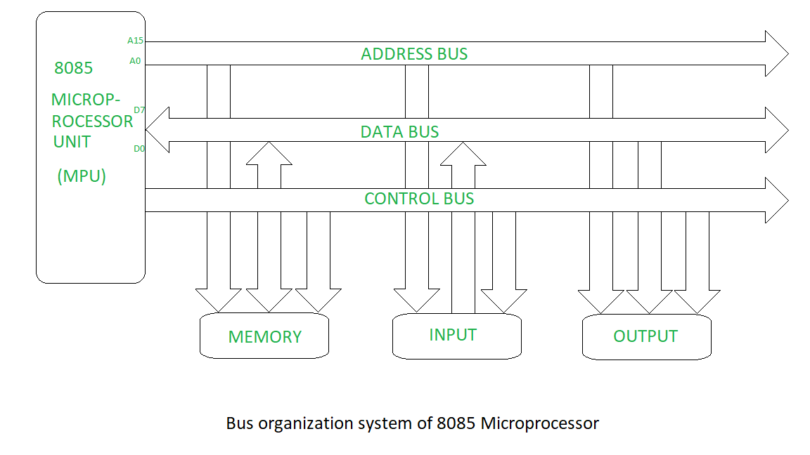
There are three types of buses.
- Address bus –
It is a group of conducting wires which carries address only.Address bus is unidirectional because data flow in one direction, from microprocessor to memory or from microprocessor to Input/output devices (That is, Out of Microprocessor). Length of Address Bus of 8085 microprocessor is 16 Bit (That is, Four Hexadecimal Digits), ranging from 0000 H to FFFF H, (H denotes Hexadecimal). The microprocessor 8085 can transfer maximum 16 bit address which means it can address 65, 536 different memory location. The Length of the address bus determines the amount of memory a system can address.Such as a system with a 32-bit address bus can address 2^32 memory locations.If each memory location holds one byte, the addressable memory space is 4 GB.However, the actual amount of memory that can be accessed is usually much less than this theoretical limit due to chipset and motherboard limitations. - Data bus –
It is a group of conducting wires which carries Data only.Data bus is bidirectional because data flow in both directions, from microprocessor to memory or Input/Output devices and from memory or Input/Output devices to microprocessor. Length of Data Bus of 8085 microprocessor is 8 Bit (That is, two Hexadecimal Digits), ranging from 00 H to FF H. (H denotes Hexadecimal). When it is write operation, the processor will put the data (to be written) on the data bus, when it is read operation, the memory controller will get the data from specific memory block and put it into the data bus. The width of the data bus is directly related to the largest number that the bus can carry, such as an 8 bit bus can represent 2 to the power of 8 unique values, this equates to the number 0 to 255.A 16 bit bus can carry 0 to 65535. - Control bus –
It is a group of conducting wires, which is used to generate timing and control signals to control all the associated peripherals, microprocessor uses control bus to process data, that is what to do with selected memory location. Some control signals are:
- Memory read
- Memory write
- I/O read
- I/O Write
- Opcode fetch
If one line of control bus may be the read/write line.If the wire is low (no electricity flowing) then the memory is read, if the wire is high (electricity is flowing) then the memory is written
Extra knowledge
Background and nomenclature
Computer systems generally consist of three main parts: the central processing unit (CPU) that processes data, memory that holds the programs and data to be processed, and I/O (input/output) devices as peripherals that communicate with the outside world. An early computer might contain a hand-wired CPU of vacuum tubes, a magnetic drum for main memory, and a punch tape and printer for reading and writing data respectively. A modern system might have a multi-core CPU, DDR4 SDRAM for memory, a solid-state drive for secondary storage, a graphics card and LCD as a display system, a mouse and keyboard for interaction, and a Wi-Fi connection for networking. In both examples, computer buses of one form or another move data between all of these devices.
In most traditional computer architectures, the CPU and main memory tend to be tightly coupled. A microprocessor conventionally is a single chip which has a number of electrical connections on its pins that can be used to select an “address” in the main memory and another set of pins to read and write the data stored at that location. In most cases, the CPU and memory share signalling characteristics and operate in synchrony. The bus connecting the CPU and memory is one of the defining characteristics of the system, and often referred to simply as the system bus.
It is possible to allow peripherals to communicate with memory in the same fashion, attaching adaptors in the form of expansion cards directly to the system bus. This is commonly accomplished through some sort of standardized electrical connector, several of these forming the expansion bus or local bus. However, as the performance differences between the CPU and peripherals varies widely, some solution is generally needed to ensure that peripherals do not slow overall system performance. Many CPUs feature a second set of pins similar to those for communicating with memory, but able to operate at very different speeds and using different protocols. Others use smart controllers to place the data directly in memory, a concept known as direct memory access. Most modern systems combine both solutions, where appropriate.
As the number of potential peripherals grew, using an expansion card for every peripheral became increasingly untenable. This has led to the introduction of bus systems designed specifically to support multiple peripherals. Common examples are the SATA ports in modern computers, which allow a number of hard drives to be connected without the need for a card. However, these high-performance systems are generally too expensive to implement in low-end devices, like a mouse. This has led to the parallel development of a number of low-performance bus systems for these solutions, the most common example being the standardized Universal Serial Bus (USB). All such examples may be referred to as peripheral buses, although this terminology is not universal.
In modern systems the performance difference between the CPU and main memory has grown so great that increasing amounts of high-speed memory is built directly into the CPU, known as a cache. In such systems, CPUs communicate using high-performance buses that operate at speeds much greater than memory, and communicate with memory using protocols similar to those used solely for peripherals in the past. These system buses are also used to communicate with most (or all) other peripherals, through adaptors, which in turn talk to other peripherals and controllers. Such systems are architecturally more similar to multicomputers, communicating over a bus rather than a network. In these cases, expansion buses are entirely separate and no longer share any architecture with their host CPU (and may in fact support many different CPUs, as is the case with PCI). What would have formerly been a system bus is now often known as a front-side bus.
Given these changes, the classical terms “system”, “expansion” and “peripheral” no longer have the same connotations. Other common categorization systems are based on the bus’s primary role, connecting devices internally or externally, PCI vs. SCSI for instance. However, many common modern bus systems can be used for both; SATA and the associated eSATA are one example of a system that would formerly be described as internal, while certain automotive applications use the primarily external IEEE 1394 in a fashion more similar to a system bus. Other examples, like InfiniBand and I²C were designed from the start to be used both internally and externally.
Internal buses
The internal bus, also known as internal data bus, memory bus, system bus or Front-Side-Bus, connects all the internal components of a computer, such as CPU and memory, to the motherboard. Internal data buses are also referred to as a local bus, because they are intended to connect to local devices. This bus is typically rather quick and is independent of the rest of the computer operations.
External buses
The external bus, or expansion bus, is made up of the electronic pathways that connect the different external devices, such as printer etc., to the computer.
Implementation
Early processors used a wire for each bit of the address width. For example, a 16-bit address bus had 16 physical wires making up the bus. As the buses became wider and lengthier, this approach became expensive in terms of the number of chip pins and board traces. Beginning with the Mostek 4096 DRAM, address multiplexing implemented with multiplexers became common. In a multiplexed address scheme, the address is sent in two equal parts on alternate bus cycles. This halves the number of address bus signals required to connect to the memory. For example, a 32-bit address bus can be implemented by using 16 lines and sending the first half of the memory address, immediately followed by the second half memory address
Accessing an individual byte frequently requires reading or writing the full bus width (a word) at once. In these instances the least significant bits of the address bus may not even be implemented – it is instead the responsibility of the controlling device to isolate the individual byte required from the complete word transmitted. This is the case, for instance, with the VESA Local Bus which lacks the two least significant bits, limiting this bus to aligned 32-bit transfers.
Historically, there were also some examples of computers which were only able to address words.
Bus network
A bus network is a network topology in which nodes are directly connected to a common linear (or branched) half-duplex link called a bus
Function
A host on a bus network is called a Station or workstation. In a bus network, every station will receive all network traffic, and the traffic generated by each station has equal transmission priority.A bus network forms a single network segment and collision domain. In order for nodes to transmit on the same bus simultaneously, they use a media access control technology such as carrier sense multiple access (CSMA) or a bus master.
If any link or segment of the bus is severed, all network transmission ceases due to signal bounce caused by the lack of a terminating resistor.
A bus network is a network topology in which nodes are directly connected to a common linear (or branched) half-duplex link called a bus
Advantages and disadvantages
Advantages
- Very easy to connect a computer or peripheral to a linear bus.
- Requires less cable length than a star topology resulting in lower costs
- The linear architecture is very simple and reliable
- It works well for small networks
- It is easy to extend by joining cable with connector or repeater
- If one node fails, it will not affect the whole network
Disadvantages
- The entire network shuts down if there is a break in the main cable or one of the T connectors break
- Large amount of packet collisions on the network, which results in high amounts of packet loss
- This topology is slow with many nodes in the network
- It is difficult to isolate any faults on the Network
Chipsets
The chipset provides a vital layer of abstraction for the processor. Instead
of the processor having to keep up with the latest hard drive standards,
graphics cards, or DRAM, it can be designed to interface only with the
chipset. The chipset then has the responsibility of understanding all
the different bus standards to be used by all the computer components.
The chipset acts as a bridge between the different bus standards; modern
chipsets typically contain two chips called the Northbridge and
Southbridge.
The Northbridge communicates with the processor and the compo-
nents requiring the highest bandwidth connections. Because this often
includes main memory, the Northbridge is sometimes called the Memory
Controller Hub (MCH). The connections of a Northbridge typically used
with the Pentium 4 or Athlon XP are shown in Fig. 2-1.
In this configuration, the processor communicates only with the
Northbridge and possibly another processor in a multiprocessor system.
This makes bus logic on the processor as simple as possible and allows
the most flexibility in what components are used with the processor. A
single processor design can be sold for use with multiple different types
of memory as long as chipsets are available to support each type.
Sometimes the Northbridge includes a built-in graphics controller as
well as providing a bus to an optional graphics card. This type of
Northbridge is called a Graphics Memory Controller Hub (GMCH).
Including a graphics controller in the Northbridge reduces costs by
avoiding the need to install a separate card, but it reduces performance

by requiring the system’s main memory to be used to store video images
rather than dedicated memory on the graphics card.
Performance can be improved with the loss of some flexibility by pro-
viding a separate connection from the processor directly to memory.
The Athlon 64 uses this configuration. Building a memory controller
directly into the processor die reduces the overall latency of memory
accesses. All other traffic is routed through a separate bus that connects
to the Northbridge chip. Because it now interacts directly only with the
graphics card, this type of Northbridge is sometimes called a graphics
tunnel (Fig. 2-2).
Whereas a direct bus from processor to memory improves perform-
ance, the processor die itself now determines which memory standards
will be supported. New memory types will require a redesign of the
processor rather than simply a new chipset. In addition, the two sepa-
rate buses to the processor will increase the total number of package pins
needed.
Another tactic for improving performance is increasing the total
memory bandwidth by interleaving memory. By providing two separate
bus interfaces to two groups of memory modules, one module can be read-
ing out data while another is receiving a new address. The total memory
store is divided among the separate modules and the Northbridge com-
bines the data from both memory channels to send to the processor. One
disadvantage of memory interleaving is a more expensive Northbridge
chip to handle the multiple connections. Another downside is that new
memory modules must be added in matching pairs to keep the number
of modules on each channel equal.

Communication with all lower-performance components is routed
through an Input output Controller Hub (ICH), also known as the
Southbridge chip. The Southbridge typically controls communication
between the processor and every peripheral except the graphics card and
main memory (Fig. 2-3). The expansion bus supports circuit boards plugged
directly into the motherboard. Peripheral buses support devices external
to the computer case. Usually a separate storage bus supports access to
hard drives and optical storage drives. To provide low-performance “legacy”
standards such as the keyboard, serial port, and parallel port, many
chipsets use a separate chip called the super I/O chip.
The main reason for dividing the functions of the processor,
Northbridge, Southbridge, and super I/O chips among separate chips is
flexibility. It allows different combinations to provide different func-
tionality. Multiple different Northbridge designs can allow a single
processor to work with different types of graphics and memory. Each
Northbridge may be compatible with multiple Southbridge chips to pro-
vide even more combinations. All of these combinations might still use
the same super I/O design to provide legacy standard support.
In recent years, transistor budgets for microprocessors have increased
to the point where the functionality of the chipset could easily be incor-
porated into the processor. This idea is often referred to as system-on-
a-chip, since it provides a single chip ready to interact with all the

common computer components. This is attractive because it requires less
physical space than a separate processor and chipset and packaging
costs are reduced. However, it makes the processor design dependent
upon the different bus standards it supports.
Supporting multiple standards requires duplicate hardware for each
standard built into the processor or supporting different versions of the
processor design. Because the microprocessor is much more expensive
to design, validate, and manufacture, it is often more efficient to place
these functions which depend upon constantly improving bus standards
on separate chips. As new bus standards become widely used, chipsets
are quickly developed to support them without affecting the design of
the microprocessor. For portable and handheld products where physi-
cal space is at a very high premium, it may be worth giving up the flex-
ibility of a separate chipset in order to reduce the number of chips on the
motherboard, but for desktop computers it seems likely that a separate
chipset is here to stay.
