by Dr. Jaydeep T. Vagh
Processor Bus
The processor bus controls how the microprocessor communicates with
the outside world. It is sometimes called the Front-Side Bus (FSB).
Early Pentium III and Athlon processors had high-speed cache memory
chips built into the processor package. Communication with these chips
was through a back-side bus, making the connection to the outside world
the front-side bus. More recent processors incorporate their cache
memory directly into the processor die, but the term front-side bus
persists. Some recent processor bus standards are listed in Table 2-1.
The Athlon XP enables two data transfers per bus clock whereas the
Pentium 4 enables four. For both processors, the number in the name
of the bus standard refers to the number of millions of transfers per
second. Because both processors perform more than one transfer per
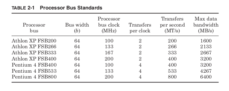
clock, neither FSB400 bus uses a 400-MHz clock, even though both are
commonly referred to as “400-MHz” buses. From a performance per-
spective this makes perfect sense. The data buses for both processors
have the same width (64 bits), so the data bandwidth at 400 MT/s is the
same regardless of the frequency of the bus clock. Both FSB400 stan-
dards provide a maximum of 3.2 GB/s data bandwidth. Where the true
bus clock frequency makes a difference is in determining the processor
frequency.
Multiplying the frequency of the bus clock by a value set by the man-
ufacturer generates the processor clock. This value is known as the bus
multiplier or bus ratio. The allowable bus ratios and the processor bus
clock frequency determine what processor frequencies are possible.
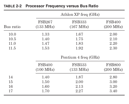
Table 2-2 shows some of these possible clock frequencies for the Athlon
XP and Pentium 4 for various bus speeds.
The Athlon XP allows for half bus ratios, so for a 200-MHz bus clock,
the smallest possible increment in processor frequency is 100 MHz. The
Pentium 4 allows only integer bus ratios, so for a 200-MHz bus clock the
smallest possible increment is 200 MHz. As processor bus ratios get
very high, performance can become more and more limited by commu-
nication through the processor bus. This is why improvements in bus
frequency are also required to steadily improve computer performance.
Of course, to run at a particular frequency the processor must not only
have the appropriate bus ratio, but also the slowest circuit path on the
processor must be faster than the chosen frequency. Before processors
are sold, their manufacturers test them to find the highest bus ratio they
can successfully run. Changes to the design or the manufacturing process
can improve the average processor frequency, but there is always some
manufacturing variation.
Like a sheet of cookies in which the cookies in the center are overdone
and those on the edge underdone, processors with identical designs that
have been through the same manufacturing process will not all run at the
same maximum frequency. An Athlon XP being sold to use FSB400 might
first be tested at 2.3 GHz. If that test fails, the same test would be repeated
at 2.2 GHz, then 2.1 GHz, and so on until a passing frequency is found,
and the chip is sold at that speed. If the minimum frequency for sale fails,
then the chip is discarded. The percentages of chips passing at each
frequency are known as the frequency bin splits, and each manufac-
turer works hard to increase bin splits in the top frequency bins since
these parts have the highest performance and are sold at the highest
prices.
To get top bin frequency without paying top bin prices, some users
overclock their processors. This means running the processor at a higher
frequency than the manufacturer has specified. In part, this is possible
because the manufacturer’s tests tend to be conservative. In testing for
frequency, they may assume a low-quality motherboard and poor cooling
and guarantee that even with continuous operation on the worst case
application the processor will still function correctly for 10 years. A
system with a very good motherboard and enhanced cooling may be
able to achieve higher frequencies than the processor specification.
Another reason some processors can be significantly overclocked is down
binning. From month to month the demand for processors from different
frequency bins may not match exactly what is produced by the fab. If
more high-frequency processors are produced than can be sold, it may be
time to drop prices, but in the meantime rather than stockpile processors
as inventory, some high-frequency parts may be sold at lower frequency
bins. Ultimately a 2-GHz frequency rating only guarantees the processor
will function at 2 GHz, not that it might not be able to go faster.
There is more profit selling a part that could run at 2.4 GHz at its full
speed rating, but selling it for less money is better than not all. Serious over-
clockers may buy several parts from the lowest frequency bin and test each
one for its maximum frequency hoping to find a very high-frequency part
that was down binned. After identifying the best one they sell the others.
Most processors are sold with the bus ratio permanently fixed. Therefore,
to overclock the processor requires increasing the processor bus clock
frequency. Because the processor derives its own internal clock from the
bus clock, at a fixed bus ratio increasing the bus clock will increase
the processor clock by the same percentage. Some motherboards allow
the user to tune the processor bus clock specifically for this purpose.
Over clockers increase the processor bus frequency until their computer
fails then decrease it a notch.
One potential problem is that the other bus clocks on the motherboard
are typically derived from the processor bus frequency. This means
increasing the processor bus frequency can increase the frequency of
not only the processor but of all the other components as well. The
frequency limiter could easily be some component besides the processor.
Some motherboards have the capability of adjusting the ratios between
the various bus clocks to allow the other buses to stay near their nominal
frequency as the processor bus is overclocked.
Processor overclocking is no more illegal than working on your own
car, and there are plenty of amateur auto mechanics who have been able
to improve the performance of their car by making a few modifications.
However, it is important to remember that overclocking will invalidate
a processor’s warranty. If a personally installed custom muffler system
causes a car to break down, it’s unlikely the dealer who sold the car
would agree to fix it.
Overclocking reduces the lifetime of the processor. Like driving a car
with the RPM in the red zone all the time, overclocked processors are
under more strain than the manufacturer deemed safe and they will
tend to wear out sooner. Of course, most people replace their computers
long before the components are worn out anyway, and the promise and
maybe more importantly the challenge of getting the most out of their
computer will continue to make overclocking a rewarding hobby for some.
Main Memory

The main memory store of computers today is always based on a partic-
ular type of memory circuit, Dynamic Random Access Memory (DRAM).
Because this has been true since the late 1970s, the terms main memory
and DRAM have become effectively interchangeable. DRAM chips provide
efficient storage because they use only one transistor to store each bit of
information.
The transistor controls access to a capacitor that is used to hold an
electric charge. To write a bit of information, the transistor is turned on
and charge is either added to or drained from the capacitor. To read, the
transistor is turned on again and the charge on the capacitor is detected
as a change in voltage on the output of the transistor. A gigabit DRAM
chip has a billion transistors and capacitors storing information.
Over time the DRAM manufacturing process has focused on creating
capacitors that will store more charge while taking up less die area. This
had led to creating capacitors by etching deep trenches into the surface
of the silicon, allowing a large capacitor to take up very little area at
the surface of the die. Unfortunately the capacitors are not perfect. Charge
tends to leak out over time, and all data would be lost in less than a
second. This is why DRAM is called a dynamic memory; the charge in
all the capacitors must be refreshed about every 15 ms
Cache memories are implemented using only transistors as Static
Random Access Memory (SRAM). SRAM is a static memory because it
will hold its value as long as power is supplied. This requires using six
transistors for each memory bit instead of only one. As a result, SRAM
memories require more die area per bit and therefore cost more per bit.
However, they provide faster access and do not require the special
DRAM processing steps used to create the DRAM cell capacitors. The
manufacturing of DRAMs has diverged from that of microprocessors; all
processors contain SRAM memories, as they normally do not use DRAM
cells.
Early DRAM chips were asynchronous, meaning there was no shared
timing signal between the memory and the processor. Later, synchronous
DRAM (SDRAM) designs used shared clocking signals to provide higher
bandwidth data transfer. All DRAM standards currently being manu-
factured use some type of clocking signal. SDRAM also takes advantage
of memory accesses typically appearing in bursts of sequential addresses.
The memory bus clock frequency is set to allow the SDRAM chips to
perform one data transfer every bus clock, but only if the transfers are
from sequential addresses. This operation is known as burst mode and
it determines the maximum data bandwidth possible. When accessing
nonsequential locations, there are added latencies. Different DRAM
innovations have focused on improving both the maximum data band-
width and the average access latency.
DRAM chips contain grids of memory cells arranged into rows and
columns. To request a specific piece of data, first the row address is sup-
plied and then a column address is supplied. The row access strobe
(RAS) and column access strobe (CAS) signals tell the DRAM whether
the current address being supplied is for a row or column. Early DRAM
designs required a new row address and column address be given for
every access, but very often the data being accessed was multiple
columns on the same row. Current DRAM designs take advantage of this
by allowing multiple accesses to the same memory row to be made with-
out the latency of driving a new row address.
After a new row is accessed, there is a delay before a column address
can be driven. This is the RAS to CAS delay (T RCD ). After the column
address is supplied, there is a latency until the first piece of data is sup-
plied, the CAS latency (T CL ). After the CAS latency, data arrives every
clock cycle from sequential locations. Before a new row can be accessed,
the current row must be precharged (T RP ) to leave it ready for future
accesses. In addition to the bus frequency, these three latencies are
used to describe the performance of an SDRAM. They are commonly
specified in the format “T CL − T RCD − T RP .” Typical values for each of these
would be 2 or 3 cycles. Thus, Fig. 2-4 shows the operation of a “2-2-3”
SDRAM.

Average latency is improved by dividing DRAM into banks where one
bank precharges while another is being accessed. This means the worst-
case latency would occur when accessing a different row in the same
bank. In this case, the old row must be precharged, then a new row
address given, and then a new column address given. The overall latency
would be T RP + T RCD + T CL .
Banking reduces the average latency because an access to a new row
in a different bank no longer requires a precharge delay. When access-
ing one bank, the other banks are precharged while waiting to be used.
So an access to a different bank has latency, T RCD + T CL . Accessing a dif-
ferent column in an already open row has only latency T CL , and sequen-
tial locations after that column address are driven every cycle. These
latencies are summarized in Table 2-3.

The double data rate SDRAM (DDR SDRAM) standard provides more
bandwidth by supplying two pieces of data per memory bus clock in
burst mode instead of just one. This concept has been extended by the
DDR2 standard that operates in the same fashion as DDR but uses dif-
ferential signaling to achieve higher frequencies. By transmitting data
as a voltage difference between two wires, the signals are less suscepti-
ble to noise and can be switched more rapidly. The downside is that two
package pins and two wires are used to transmit a single bit of data.
Rambus DRAM (RDRAM) achieves even higher frequencies by plac-
ing more constraints on the routing of the memory bus and by limiting
the number of bits in the bus. The more bits being driven in parallel,
the more difficult it is to make sure they all arrive at the same moment.
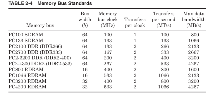
As a result, many bus standards are shifting toward smaller numbers
of bits driven at higher frequencies. Some typical memory bus stan-
dards are shown in Table 2-4.
To make different DRAM standards easier to identify, early SDRAM
standards were named “PC#” where the number stood for the bus fre-
quency, but the advantage of DDR is in increased bandwidth at the same
frequency, so the PC number was used to represent total data band-
width instead. Because of the confusion this causes, DDR and DDR2
memory are often also named by the number of data transfers per second.
Just as with processor buses, transfers per cycle and clocks per cycle
are often confused, and this leads to DDR266 being described as 266-MHz
memory even though its clock is really only half that speed. As if things
weren’t confusing enough, the early RDRAM standards used the PC
number to represent transfers per cycle, while later wider RDRAM bus
standards have changed to being labeled by total bandwidth like DDR
memory.
Suffice it to say that one must be very careful in buying DRAM to make
sure to get the appropriate type for your computer. Ideally, the memory bus
standard will support the same maximum bandwidth as the processor bus.
This allows the processor to consume data at its maximum rate without
wasting money on memory that is faster than your processor can use.

Various memory modules containing different types of DRAM (from top to bottom): DDR SDRAM, SDRAM, EDO DRAM, and FPM DRAM
Video Adapters (Graphics Cards)

A video card (also called a display card, graphics card, display adapter, or graphics adapter) is an expansion card which generates a feed of output images to a display device (such as a computer monitor). Frequently, these are advertised as discrete or dedicated graphics cards, emphasizing the distinction between these and integrated graphics. At the core of both is the graphics processing unit (GPU), which is the main part that does the actual computations, but should not be confused as the video card as a whole, although “GPU” is often used to refer to video cards.
Most output devices consume data at a glacial pace compared with the
processor’s ability to produce it. The most important exception is the
video adapter and display. A single high-resolution color image can con-
tain 7 MB of data and at a typical computer monitor refresh rate of
72 Hz, the display could output data at more than 500 MB/s. If multiple
frames are to be combined or processed into one, even higher data rates
could be needed. Because of the need for high data bandwidth, the video
adapter that drives the computer monitor typically has a dedicated
high-speed connection to the Northbridge of the chipset.
Early video adapters simply translated the digital color images pro-
duced by the computer to the analog voltage signals that control the
monitor. The image to be displayed is assembled in a dedicated region
of memory called the frame buffer. The amount of memory required for
the frame buffer depends on the resolution to be displayed and the
number of bits used to represent the color of each pixel.
Typical resolutions range anywhere from 640 × 480 up to 1600 × 1200,
and color is specified with 16, 24, or 32 bits. A display of 1600 × 1200 with
32-bit color requires a 7.3 MB frame buffer (7.3 = 1600 × 1200 × 32/2 20 ).
The Random Access Memory Digital-to-Analog Converter (RAMDAC)
continuously scans the frame buffer and converts the binary color of each
pixel to three analog voltage signals that drive the red, green, and blue
monitor controls.
Double buffering allocates two frame buffers, so that while one frame
is being displayed, the next is being constructed. The RAMDAC alter-
nates between the two buffers, so that one is always being read and one is
always being written. To help generate 3D effects a z-buffer may also be
used. This is a block of memory containing the effective depth (or z-value)
of each pixel in the frame buffer. The z-buffer is used to determine what
part of each new polygon should be drawn because it is in front of the
other polygons already drawn.
Texture maps are also stored in memory to be used to color surfaces
in 3D images. Rather than trying to draw the coarse surface of a brick
wall, the computer renders a flat surface and then paints the image with
a brick texture map. The sky in a 3D game would typically not be mod-
eled as a vast open space with 3D clouds moving through it; instead it
would be treated as a flat ceiling painted with a “sky” texture map.


Storing and processing all this data could rapidly use up the com-
puter’s main memory space and processing power. To prevent this all
modern video adapters are also graphics accelerators, meaning they
contain dedicated graphics memory and a graphics processor. The
memory used is the same DRAM chips used for main memory or slight
variations. Graphics accelerators commonly come with between 1 and
32 MB of memory built in.
The Graphics Processor Unit (GPU) can off-load work from the Central
Processing Unit (CPU) by performing many of the tasks used in creat-
ing 2D or 3D images. To display a circle without a graphics processor,
the CPU might create a bitmap containing the desired color of each
pixel and then copy it into the frame buffer. With a graphics processor,
the CPU might issue a command to the graphics processor asking for a
circle with a specific color, size, and location. The graphics processor
would then perform the task of deciding the correct color for each pixel.
Modern graphics processors also specialize in the operations required
to create realistic 3D images. These include shading, lighting, reflections,
transparency, distance fogging, and many others. Because they contain
specialized hardware, the GPUs perform these functions much more
quickly than a general-purpose microprocessor. As a result, for many of
the latest 3D games the performance of the graphics accelerator is more
important than that of the CPU.
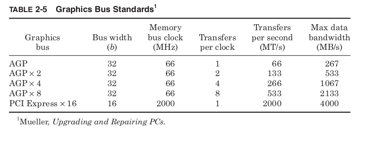
The most common bus interfaces between the video adapter and the
Northbridge are the Accelerated Graphics Port (AGP) standards. The
most recent standards, PCI Express, began to be used in 2004. These
graphics bus standards are shown in Table 2-5.
Some chipsets contain integrated graphics controllers. This means the
Northbridge chips include a graphics processor and video adapter, so that
a separate video adapter card is not required. The graphics performance
of these built-in controllers is typically less than the latest separate video
cards. Lacking separate graphics memory, these integrated controllers
must use main memory for frame buffers and display information. Still,
for systems that are mainly used for 2D applications, the graphics
provided by these integrated solutions is often more than sufficient,
and the cost savings are significant.
Dedicated vs integrated graphics
Classical desktop computer architecture with a distinct graphics card over PCI Express. Typical bandwidths for given memory technologies, missing are the memory latency. Zero-copy between GPU and CPU is not possible, since both have their distinct physical memories. Data must be copied from one to the other to be shared.
Integrated graphics with partitioned main memory: a part of the system memory is allocated to the GPU exclusively. Zero-copy is not possible, data has to be copied, over the system memory bus, from one partition to the other.
Integrated graphics with unified main memory, to be found AMD “Kaveri” or PlayStation 4 (HSA).
As an alternative to the use of a video card, video hardware can be integrated into the motherboard, CPU, or a system-on-chip. Both approaches can be called integrated graphics. Motherboard-based implementations are sometimes called “on-board video”. Almost all desktop computer motherboards with integrated graphics allow the disabling of the integrated graphics chip in BIOS, and have a PCI, or PCI Express (PCI-E) slot for adding a higher-performance graphics card in place of the integrated graphics. The ability to disable the integrated graphics sometimes also allows the continued use of a motherboard on which the on-board video has failed. Sometimes both the integrated graphics and a dedicated graphics card can be used simultaneously to feed separate displays. The main advantages of integrated graphics include cost, compactness, simplicity and low energy consumption. The performance disadvantage of integrated graphics arises because the graphics processor shares system resources with the CPU. A dedicated graphics card has its own random access memory (RAM), its own cooling system, and dedicated power regulators, with all components designed specifically for processing video images. Upgrading to a dedicated graphics card offloads work from the CPU and system RAM, so not only will graphics processing be faster, but the computer’s overall performance may also improve.
Both AMD and Intel have introduced CPUs and motherboard chipsets which support the integration of a GPU into the same die as the CPU. AMD markets CPUs with integrated graphics under the trademark Accelerated Processing Unit (APU), while Intel markets similar technology under the “Intel HD Graphics and Iris” brands. With the 8th Generation Processors, Intel announced the Intel UHD series of Integrated Graphics for better support of 4K Displays.[6] Although they are still not equivalent to the performance of discrete solutions, Intel’s HD Graphics platform provides performance approaching discrete mid-range graphics, and AMD APU technology has been adopted by both the PlayStation 4 and Xbox One video game consoles.
Power demand
As the processing power of video cards has increased, so has their demand for electrical power. Current high-performance video cards tend to consume a great deal of power. For example, the thermal design power (TDP) for the GeForce GTX TITAN is 250 watts.When tested while gaming, the GeForce GTX 1080 Ti Founder’s Edition averaged 227 watts of power consumption.[11] While CPU and power supply makers have recently moved toward higher efficiency, power demands of GPUs have continued to rise, so video cards may have the largest power consumption in a computer. Although power supplies are increasing their power too, the bottleneck is due to the PCI-Express connection, which is limited to supplying 75 watts.Modern video cards with a power consumption of over 75 watts usually include a combination of six-pin (75 W) or eight-pin (150 W) sockets that connect directly to the power supply. Providing adequate cooling becomes a challenge in such computers. Computers with multiple video cards may need power supplies in the 1000–1500 W range. Heat extraction becomes a major design consideration for computers with two or more high-end video cards.
3D graphic APIs
A graphics driver usually supports one or multiple cards by the same vendor, and has to be specifically written for an operating system. Additionally, the operating system or an extra software package may provide certain programming APIs for applications to perform 3D rendering.
| OS | Vulkan | Direct X | GNMX | Metal | OpenGL | OpenGL ES |
|---|---|---|---|---|---|---|
| Windows 10 | Nvidia/AMD | Microsoft | No | No | Yes | Yes |
| macOS | MoltenVK | No | No | Apple | Apple | No |
| GNU/Linux | Yes | No | No | No | Yes | Yes |
| Android | Yes | No | No | No | Nvidia | Yes |
| iOS | MoltenVK | No | No | Apple | No | Apple |
| Tizen | In development | No | No | No | No | Yes |
| Sailfish | In development | No | No | No | No | Yes |
| Xbox One | No | Yes | No | No | No | No |
| Orbis OS (PS4) | No | No | Yes | No | No | No |
| Nintendo Switch | Yes | No | No | No | Yes | Yes |
table is a comparison between a selection of the features of some of those interfaces.
| Bus | Width (bits) | Clock rate (MHz) | Bandwidth (MB/s) | Style |
|---|---|---|---|---|
| ISA XT | 8 | 4.77 | 8 | Parallel |
| ISA AT | 16 | 8.33 | 16 | Parallel |
| MCA | 32 | 10 | 20 | Parallel |
| NUBUS | 32 | 10 | 10–40 | Parallel |
| EISA | 32 | 8.33 | 32 | Parallel |
| VESA | 32 | 40 | 160 | Parallel |
| PCI | 32–64 | 33–100 | 132–800 | Parallel |
| AGP 1x | 32 | 66 | 264 | Parallel |
| AGP 2x | 32 | 66 | 528 | Parallel |
| AGP 4x | 32 | 66 | 1000 | Parallel |
| AGP 8x | 32 | 66 | 2000 | Parallel |
| PCIe x1 | 1 | 2500 / 5000 | 250 / 500 | Serial |
| PCIe x4 | 1 × 4 | 2500 / 5000 | 1000 / 2000 | Serial |
| PCIe x8 | 1 × 8 | 2500 / 5000 | 2000 / 4000 | Serial |
| PCIe x16 | 1 × 16 | 2500 / 5000 | 4000 / 8000 | Serial |
| PCIe x1 2.0[41] | 1 | 500 / 1000 | Serial | |
| PCIe x4 2.0 | 1 x 4 | 2000 / 4000 | Serial | |
| PCIe x8 2.0 | 1 x 8 | 4000 / 8000 | Serial | |
| PCIe x16 2.0 | 1 × 16 | 5000 / 10000 | 8000 / 16000 | Serial |
| PCIe X1 3.0 | 1 | 1000 / 2000 | Serial | |
| PCIe X4 3.0 | 1 x 4 | 4000 / 8000 | Serial | |
| PCIe X8 3.0 | 1 x 8 | 8000 / 16000 | Serial | |
| PCIe X16 3.0 | 1 x 16 | 16000 / 32000 | Serial |
Storage Devices
Because hard drives are universally used by computers as primary stor-
age, Southbridge chips of most chipsets have a bus specifically intended
for use with hard drives. Hard drives store binary data as magnetic dots
on metal platters that are spun at high speeds to allow the drive head
to read or to change the magnetic orientation of the dots passing beneath.
Hard drives have their own version of Moore’s law based not on shrink-
ing transistors but on shrinking the size of the magnetic dots used to store
data. Incredibly they have maintained the same kind of exponential
trend of increasing densities over the same time period using funda-
mentally different technologies from computer chip manufacturing. By
steadily decreasing the area required for a single magnetic dot, the hard
drive industry has provided steadily more capacity at lower cost. This
trend of rapidly increasing storage capacity has been critical in making
use of the rapidly increasing processing capacity of microprocessors.
More tightly packed data and higher spin rates have also increased the
maximum data transfer bandwidth drives support. This has created the
need for higher bandwidth storage bus standards shown in Table 2-6.
The most common storage bus standard is Advanced Technology
Attachment (ATA). It was used with the first hard drives to include

built-in controllers, so the earliest version of ATA is usually referred to
by the name Integrated Drive Electronics (IDE). Later increases
in bandwidth were called Enhanced IDE (EIDE) and Ultra-ATA. The
most common alternative to ATA is Small Computer System Interface
(SCSI pronounced “scuzzy”). More commonly used in high performance
PC servers than desktops, SCSI drives are also often used with Macintosh
computers. Increasing the performance of the fastest ATA or SCSI bus
standards becomes difficult because of the need to synchronize all the
data bits on the bus and the electromagnetic interference between the
different signals.
Beginning in 2004, a competing solution is Serial ATA (SATA), which
transmits data only a single bit at a time but at vastly higher clock fre-
quencies, allowing higher overall bandwidth. To help keep sender and
receiver synchronized at such high frequencies the data is encoded to
guarantee at least a single voltage transition for every 5 bits. This
means that in the worst case only 8 of every 10 bits transmitted represent
real data. The SATA standard is physically and electrically completely
different from the original ATA standards, but it is designed to be soft-
ware compatible.
Although most commonly used with hard drives, any of these stan-
dards can also be used with high-density floppy drives, tape drives, or
optical CD or DVD drives. Floppy disks and tape drives store data mag-
netically just as hard drives do but use flexible media. This limits the
data density but makes them much more affordable as removable media.
Tapes store vastly more than disks by allowing the media to wrap upon
itself, at the cost of only being able to efficiently access the data serially.
Optical drives store information as pits in a reflective surface that are
read with a laser. As the disc spins beneath a laser beam, the reflection
flashes on and off and is read by a photodetector like a naval signal light.
CDs and DVDs use the same mechanism, with DVDs using smaller,
more tightly packed pits. This density requires DVDs to use a shorter-
wavelength laser light to accurately read the smaller pits.
A variety of writable optical formats are now available. The CD-R
and DVD-R standards allow a disc to be written only once by heating a dye
in the disc with a high-intensity laser to make the needed nonreflective
dots. The CD-RW and DVD-RW standards allow discs to be rewritten
by using a phase change media. A high-intensity laser pulse heats a spot
on the disc that is then either allowed to rapidly cool or is repeatedly
heated at lower intensity causing the spot to cool gradually. The phase
change media will freeze into a highly reflective or a nonreflective form
depending on the rate it cools. Magneto-optic (MO) discs store information
magnetically but read it optically. Spots on the disc reflect light with a
different polarization depending on the direction of the magnetic field.
This field is very stable and can’t be changed at room temperature, but
heating the spot with a laser allows the field to be changed and the drive
to be written.
All of these storage media have very different physical mechanisms
for storing information. Shared bus standards and hardware device
drivers allow the chipset to interact with them without needing the
details of their operation, and the chipset allows the processor to be
oblivious to even the bus standards being used.
Expansion Cards
” In computing, the expansion card, expansion board, adapter card or accessory card is a printed circuit board that can be inserted into an electrical connector, or expansion slot, on a computer motherboard, backplane or riser card to add functionality to a computer system via the expansion bus. “

To allow computers to be customized more easily, almost all mother-
boards include expansion slots that allow new circuit boards to be
plugged directly into the motherboard. These expansion cards provide
higher performance than features already built into the motherboard,
or add entirely new functionality. The connection from the expansion
cards to the chipset is called the expansion bus or sometimes the
input/output (I/O) bus.
In the original IBM PC, all communication internal to the system
box occurred over the expansion bus that was connected directly to the
processor and memory, and ran at the same clock frequency as the
processor. There were no separate processor, memory, or graphics buses.
In these systems, the expansion bus was simply “The Bus,” and the
original design was called Industry Standard Architecture (ISA). Some
mainstream expansion bus standards are shown in Table 2-7.
The original ISA standard transmitted data 8 bits at a time at a frequency
of 4.77 MHz. This matched the data bus width and clock frequency of the
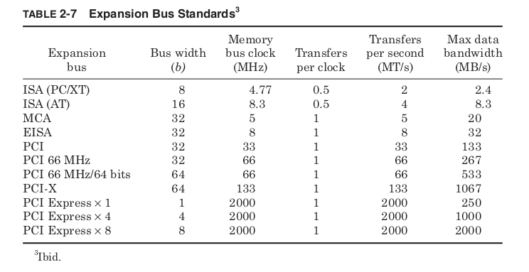
Intel 8088 processors used in the first IBM PC. Released in 1984, the
IBM AT used the Intel 286 processor. The ISA bus was expanded to
match the 16-bit data bus width of that processor and its higher clock
frequency. This 16-bit version was also backward compatible with 8-bit
cards and became enormously popular. IBM did not try to control the
ISA standard and dozens of companies built IBM PC clones and ISA
expansion cards for PCs. Both 8- and 16-bit ISA cards were still widely
used into the late 1990s.
With the release of the Intel 386, which transferred data 32 bits at a
time, it made sense that “The Bus” needed to change again. In 1987, IBM
proposed a 32-bit-wide standard called Micro Channel Architecture
(MCA), but made it clear that any company wishing to build MCA com-
ponents or computers would have to pay licensing fees to IBM. Also, the
MCA bus would not allow the use of ISA cards. This was a chance for IBM
to regain control of the PC standard it had created and time for compa-
nies that had grown rich making ISA components to pay IBM its due.
Instead, a group of seven companies led by Compaq, the largest PC
clone manufacturer at the time, created a separate 32-bit bus standard
called Extended ISA (EISA). EISA would be backward compatible with
older 8 and 16-bit ISA cards, and most importantly no licensing fees
would be charged. As a result, the MCA standard was doomed and never
appeared outside of IBM’s own PS/2 ® line. EISA never became popular
either, but the message was clear: the PC standard was now bigger than
any one company, even the original creator, IBM.
The Peripheral Component Interconnect (PCI) standard was proposed
in 1992 and has now replaced ISA. PCI offers high bandwidth but per-
haps more importantly supports Plug-n-Play (PnP) functionality. ISA
cards required the user to set switches on each card to determine which
interrupt line the card would use as well as other system resources. If
two cards tried to use the same resource, the card might not function,
and in some cases the computer wouldn’t be able to boot successfully.
The PCI standard includes protocols that allow the system to poll for new
devices on the expansion bus each time the system is started and dynam-
ically assign resources to avoid conflicts. Updates to the PCI standard
have allowed for steadily more bandwidth.
Starting in 2004, systems began appearing using PCI-Express, which
cuts the number of data lines but vastly increases frequencies. PCI-
Express is software compatible with PCI and expected to gradually
replace it. The standard allows for bus widths of 1, 4, 8, or 16 bits to allow
for varying levels of performance. Eventually PCI-Express may replace
other buses in the system. Already some systems are replacing the AGP
graphics bus with 16-bit-wide PCI-Express.
As users continue to put computers to new uses, there will always be
a need for a high-performance expansion bus.
Daughterboard

A daughterboard, daughtercard, mezzanine board or piggyback board is an expansion card that attaches to a system directly. Daughterboards often have plugs, sockets, pins or other attachments for other boards. Daughterboards often have only internal connections within a computer or other electronic devices, and usually access the motherboard directly rather than through a computer bus.
Daughterboards are sometimes used in computers in order to allow for expansion cards to fit parallel to the motherboard, usually to maintain a small form factor. This form are also called riser cards, or risers. Daughterboards are also sometimes used to expand the basic functionality of an electronic device, such as when a certain model has features added to it and is released as a new or separate model. Rather than redesigning the first model completely, a daughterboard may be added to a special connector on the main board. These usually fit on top of and parallel to the board, separated by spacers or standoffs, and are sometimes called mezzanine cards due to being stacked like the mezzanine of a theatre. Wavetable cards (sample-based synthesis cards) are often mounted on sound cards in this manner.
Some mezzanine card interface standards include the 400 pin FPGA Mezzanine Card (FMC); the 172 pin High Speed Mezzanine Card (HSMC);the PCI Mezzanine Card (PMC); XMC mezzanines; the Advanced Mezzanine Card; IndustryPacks (VITA 4), the GreenSpring Computers Mezzanine modules; etc.
Examples of daughterboard-style expansion cards include:
- Enhanced Graphics Adapter piggyback board, adds memory beyond 64 KB, up to 256 KB
- Expanded memory piggyback board, adds additional memory to some EMS and EEMS boards
- ADD daughterboard
- RAID daughterboard
- Network interface controller (NIC) daughterboard
- CPU Socket daughterboard
- Bluetooth daughterboard
- Modem daughterboard
- AD/DA/DIO daughter-card
- Communication daughterboard (CDC)
- Server Management daughterboard (SMDC)
- Serial ATA connector daughterboard
- Robotic daughterboard
- Access control List daughterboard
- Arduino “shield” daughterboards
- Beaglebone “cape” daughterboard
- Raspberry Pi “HAT” daughterboard.
- Network Daughterboard (NDB). Commonly integrates: bus interfaces logic, LLC, PHY and Magnetics onto a single board.

Peripheral Bus
In computing, a peripheral bus is a computer bus designed to support computer peripherals like printers and hard drives. The term is generally used to refer to systems that offer support for a wide variety of devices, like Universal Serial Bus, as opposed to those that are dedicated to specific types of hardware. Serial AT Attachment, or SATA is designed and optimized for communication with mass storage devices.
For devices that cannot be placed conveniently inside the computer case
and attached to the expansion bus, peripheral bus standards allow
external components to communicate with the system.
The original IBM PC was equipped with a single bidirectional bus that
transmitted a single bit of data at a time and therefore was called the
serial port (Table 2-8). In addition, a unidirectional 8-bit-wide bus
became known as the parallel port; it was primarily used for con-
necting to printers. Twenty years later, most PCs are still equipped
with these ports, and they are only very gradually being dropped from
new systems.
In 1986, Apple computer developed a dramatically higher-performance
peripheral bus, which they called FireWire. This was standardized in
1995 as IEEE standard #1394. FireWire was a huge leap forward.
Like the SATA and PCI-Express standards that would come years later,
FireWire provided high bandwidth by transmitting data only a single
bit at a time but at high frequencies. This let it use a very small phys-
ical connector, which was important for small electronic peripherals.
FireWire supported Plug-n-Play capability and was also hot swappable,
meaning it did not require a computer to be reset in order to find a new
device. Finally, FireWire devices could be daisy chained allowing any
FireWire device to provide more FireWire ports. FireWire became
ubiquitous among digital video cameras and recorders.
Meanwhile, a group of seven companies lead by Intel released their
own peripheral standard in 1996, Universal Serial Bus (USB). USB is
in many ways similar to FireWire. It transmits data serially, supports
Plug-n-Play, is hot swappable, and allows daisy chaining. However, the
original USB standard was intended to be used with low-performance,
low-cost peripherals and only allowed 3 percent of the maximum band-
width of FireWire.

In 1998, Intel began negotiations with Apple to begin including
FireWire support in Intel chipsets. FireWire would be used to support
high-performance peripherals, and USB would support low-performance
devices. Apple asked for a $1 licensing fee per FireWire connection, and
the Intel chipset that was to support FireWire was never sold. 5 Instead,
Intel and others began working on a higher-performance version of
USB. The result was the release of USB 2.0 in 2000. USB 2.0 retains
all the features of the original standard, is backward compatible, and
increases the maximum bandwidth possible to greater than FireWire at
the time. Standard with Intel chipsets, USB 2.0 is supported by most
PCs sold after 2002.
Both USB and FireWire are flexible enough and low cost enough to
be used by dozens of different devices. External hard drives and optical
drives, digital cameras, scanners, printers, personal digital assistants,
and many others use one or both of these standards. Apple has contin-
ued to promote FireWire by updating the standard (IEEE-1394b) to
allow double the bandwidth and by dropping the need to pay license fees.
In 2005, it remains to be seen if USB or FireWire will eventually replace
the other. For now, it seems more likely that both standards will be
supported for some years to come, perhaps until some new as yet
unformed standard replaces them both.
Motherboards
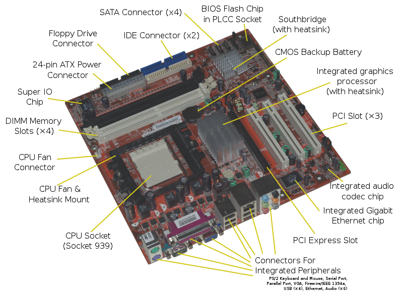
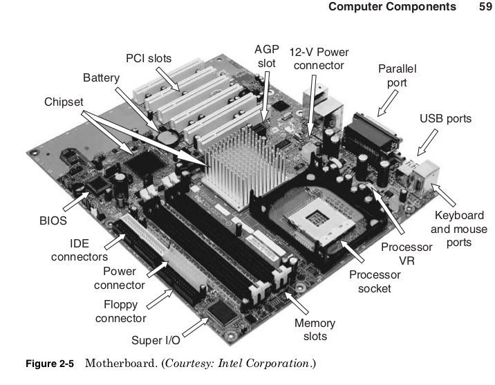
A motherboard (sometimes alternatively known as the mainboard, main circuit board, system board, baseboard, planar board or logic board,[1] or colloquially, a mobo) is the main printed circuit board (PCB) found in general purpose computers and other expandable systems. It holds and allows communication between many of the crucial electronic components of a system, such as the central processing unit (CPU) and memory, and provides connectors for other peripherals. Unlike a backplane, a motherboard usually contains significant sub-systems such as the central processor, the chipset’s input/output and memory controllers, interface connectors, and other components integrated for general purpose use and applications.
The motherboard is the circuit board that connects the processor,
chipset, and other computer components, as shown in Fig. 2-5. It phys-
ically implements the buses that tie these components together and
provides all their physical connectors to the outside world.
The chipset used is the most important choice in the design of a mother-
board. This determines the available bus standards and therefore the
type of processor, main memory, graphics cards, storage devices, expan-
sions cards, and peripherals the motherboard will support.
For each chip to be used on the motherboard, a decision must be made
whether to solder the chip directly to the board or provide a socket that
it can be plugged into. Sockets are more expensive but leave open the
possibility of replacing or upgrading chips later. Microprocessors and
DRAM are the most expensive required components, and therefore are
typically provided with sockets. This allows a single motherboard design
to be used with different processor designs and speeds, provided they
are available in a compatible package. Slots for memory modules also
allow the speed and total amount of main memory to be customized.
The chipset determines the types of expansion slots available, and the
physical size (or form factor) of the board limits how many are provided.
Some common form factors are shown in Table 2-9.
By far the most common form factor for motherboards is the Advanced
Technology Extended (ATX) standard. ATX motherboards come in four
different sizes, with the main difference being that the smaller boards
offer fewer expansion slots. All the ATX sizes are compatible, meaning
that they use the same power supply connectors and place mounting
holes in the same places. This means a PC case and power supply
designed for any of the ATX sizes can be used with that size or any of
the smaller ATX standards.

In 2004, motherboards using the Balanced Technology Extended
(BTX) standard began appearing. This new standard is incompatible
with ATX and requires new cases although it does use the same power
supply connectors. The biggest change with the BTX standard is rear-
ranging the placement of the components on the board to allow for
improved cooling. When the ATX standard first came into use, the cool-
ing of the components on the motherboard was not a serious consider-
ation. As processor power increased, large heavy heat sinks with
dedicated fans became required.
More recently, chipsets and graphics cards have begun requiring their
own heat sinks and fans. The performance possible from these compo-
nents can be limited by the system’s ability to cool them, and adding
more fans or running the fans at higher speed may quickly create an
unacceptable level of noise.
The BTX standard lines up the processor, chipset, and graphics card,
so air drawn in from a single fan at the front of the system travels in a
straight path over all these components and out the back of the system.
This allows fewer total fans and slower fan speeds, making BTX systems
quieter than ATX systems providing the same level of cooling. Like ATX,
the different BTX standards are compatible, with cases designed for one
BTX board accommodating any smaller BTX size.
Processor performance can be limited not only by the ability to pull heat
out but also by the ability of the motherboard to deliver power into the
processor. The power supply of the case converts the AC voltage of a wall
socket to standard DC voltages: 3.3, 5, and 12 V. However, the processor
itself may require a different voltage. The motherboard Voltage Regulator
(VR) converts the standard DC voltages into the needed processor voltage.
Early motherboards required switches to be set to determine the volt-
age delivered by the VR, but this created the risk of destroying your
processor by accidentally running it at very high voltage. Modern proces-
sors use voltage identification (VID) to control the voltage produced by
the VR. When the system is first turned on, the motherboard powers a
small portion of the microprocessor with a fixed voltage. This allows the
processor to read built-in fuses specifying the proper voltage as deter-
mined by the manufacturer. This is signaled to the VR, which then
powers up the rest of the processor at the right voltage.
Microprocessor power can be over 115 W at voltages as low as 1.4 V,
requiring the VR to supply 80 A of current or more. The VR is actually
not a single component but a collection of power transistors, capacitors,
and inductors. The VR constantly monitors the voltage it is providing
to the processor and turns power transistors on and off to keep within
a specified tolerance of the desired voltage. The capacitors and induc-
tors help reduce noise on the voltage supplied by the VR.
If the VR cannot react quickly enough to dips or spikes in the proces-
sor’s current draw, the processor may fail or be permanently damaged.
The large currents and fast switching of the VR transistors cause them
to become yet another source of heat in the system. Limiting the max-
imum current they can supply will reduce VR heat and cost, but this may
limit the performance of the processor.
To reduce average processor and VR power and extend battery life in
portable products, some processors use VID to dynamically vary their
voltage. Because the processor controls its own voltage through the VID
signals to the VR, it can reduce its voltage to save power. A lower volt-
age requires running at a lower frequency, so this would typically only
be done when the system determines that maximum performance is
not currently required. If the processor workload increases, the voltage
and frequency are increased back to their maximum levels. This is the
mechanism behind Transmeta’s LongRun ® , AMD’s PowerNow! ® , and
Intel’s Enhanced SpeedStep ® technologies.
A small battery on the motherboard supplies power to a Real Time
Clock (RTC) counter that keeps track of the passage of time when the
system is powered down. The battery also supplies power to a small
memory called the CMOS RAM that stores system configuration infor-
mation. The name CMOS RAM is left over from systems where the
processor and main memory were made using only NMOS transistors,
and the CMOS RAM was specially made to use NMOS and PMOS,
which allowed it to have extremely low standby power. These days all
the chips on the motherboard are CMOS, but the name CMOS RAM per-
sists. Modern chipsets will often incorporate both the real time clock
counter and CMOS RAM into the Southbridge chip.
To create clock signals to synchronize all the motherboard compo-
nents, a quartz crystal oscillator is used. A small sliver of quartz has a
voltage applied to it that causes it to vibrate and vary the voltage signal
at a specific frequency. The original IBM PC used a crystal with a fre-
quency of 14.318 MHz, and all PC motherboards to this day use a crys-
tal with the same frequency. Multiplying or dividing the frequency of this
one crystal creates almost all the clock signals on all the chips in the com-
puter system. One exception is a separate crystal with a frequency of
32.768 kHz, which is used to drive the RTC. This allows the RTC to count
time independent of the speed of the buses and prevents an overclocked
system from measuring time inaccurately.
The complexity of motherboards and the wide variety of components
they use make it difficult to write software to interact directly with
more than one type of motherboard. To provide a standard software
interface every motherboard provides basic functions through its own
Basic Input Output System (BIOS).
Design
A motherboard provides the electrical connections by which the other components of the system communicate. Unlike a backplane, it also contains the central processing unit and hosts other subsystems and devices.
A typical desktop computer has its microprocessor, main memory, and other essential components connected to the motherboard. Other components such as external storage, controllers for video display and sound, and peripheral devices may be attached to the motherboard as plug-in cards or via cables; in modern microcomputers it is increasingly common to integrate some of these peripherals into the motherboard itself.
An important component of a motherboard is the microprocessor’s supporting chipset, which provides the supporting interfaces between the CPU and the various buses and external components. This chipset determines, to an extent, the features and capabilities of the motherboard.
Modern motherboards include:
- Sockets (or slots) in which one or more microprocessors may be installed. In the case of CPUs in ball grid array packages, such as the VIA C3, the CPU is directly soldered to the motherboard.
- Memory Slots into which the system’s main memory is to be installed, typically in the form of DIMM modules containing DRAM chips
- A chipset which forms an interface between the CPU’s front-side bus, main memory, and peripheral buses
- Non-volatile memory chips (usually Flash ROM in modern motherboards) containing the system’s firmware or BIOS
- A clock generator which produces the system clock signal to synchronize the various components
- Slots for expansion cards (the interface to the system via the buses supported by the chipset)
- Power connectors, which receive electrical power from the computer power supply and distribute it to the CPU, chipset, main memory, and expansion cards. As of 2007, some graphics cards (e.g. GeForce 8 and Radeon R600) require more power than the motherboard can provide, and thus dedicated connectors have been introduced to attach them directly to the power supply.
- Connectors for hard drives, typically SATA only. Disk drives also connect to the power supply.
Additionally, nearly all motherboards include logic and connectors to support commonly used input devices, such as USB for mouse devices and keyboards. Early personal computers such as the Apple II or IBM PC included only this minimal peripheral support on the motherboard. Occasionally video interface hardware was also integrated into the motherboard; for example, on the Apple II and rarely on IBM-compatible computers such as the IBM PC Jr. Additional peripherals such as disk controllers and serial ports were provided as expansion cards.
Given the high thermal design power of high-speed computer CPUs and components, modern motherboards nearly always include heat sinks and mounting points for fans to dissipate excess heat.

