by Dr. Jaydeep T. Vagh
Basic Input Output System
Today Microsoft Windows comes with dozens of built-in applications from
Internet Explorer to Minesweeper, but at its core the primary function of
the operating system is still to load and run programs. However, the oper-
ating system itself is a program, which leads to a “chicken-and-egg” prob-
lem. If the operating system is used to load programs, what loads the
operating system? After the system is powered on the processor’s memory
state and main memory are both blank. The processor has no way of
knowing what type of motherboard it is in or how to load an operating
system. The Basic Input Output System (BIOS) solves this problem.
After resetting itself, the very first program the processor runs is the
BIOS. This is stored in a flash memory chip on the motherboard called
the BIOS ROM. Using flash memory allows the BIOS to be retained even
when the power is off. The first thing the BIOS does is run a Power-On
Self-Test (POST) check. This makes sure the most basic functions of the
motherboard are working. The BIOS program then reads the CMOS
RAM configuration information and allows it to be modified if prompted.
Finally, the BIOS runs a bootstrap loader program that searches for an
operating system to load.
In order to display information on the screen during POST and be able
to access storage devices that might hold the operating system, the
BIOS includes device drivers. These are programs that provide a stan-
dard software interface to different types of hardware. The drivers are
stored in the motherboard BIOS as well as in ROM chips built into
hardware that may be used during the boot process, such as video
adapters and disk drives.
As the operating system boots, one of the first things it will do is load
device drivers from the hard drive into main memory for all the hard-
ware that did not have device drivers either in the motherboard BIOS
or built-in chips. Most operating systems will also load device drivers
to replace all the drivers provided by the BIOS with more sophisticated
higher-performance drivers. As a result, the BIOS device drivers are typ-
ically only used during the system start-up but still play a crucial role.
The drivers stored on a hard drive couldn’t be loaded without at least a
simple BIOS driver that allows the hard drive to be read in the first place.
In addition to the first few seconds of start-up, the only time Windows
XP users will actually be using the BIOS device drivers is when boot-
ing Windows in “safe” mode. If a malfunctioning driver is loaded by the
operating system, it may prevent the user from being able to load the
proper driver. Booting in safe mode causes the operating system to not
load it own drivers and to rely upon the BIOS drivers instead. This
allows problems with the full boot sequence to be corrected before return-
ing to normal operation.
By providing system initialization and the first level of hardware abstrac-
tion, the BIOS forms a key link between the hardware and software.
Memory Hierarchy
Memory Hierarchy Design and its Characteristics
In the Computer System Design, Memory Hierarchy is an enhancement to organize the memory such that it can minimize the access time. The Memory Hierarchy was developed based on a program behavior known as locality of references.The figure below clearly demonstrates the different levels of memory hierarchy :
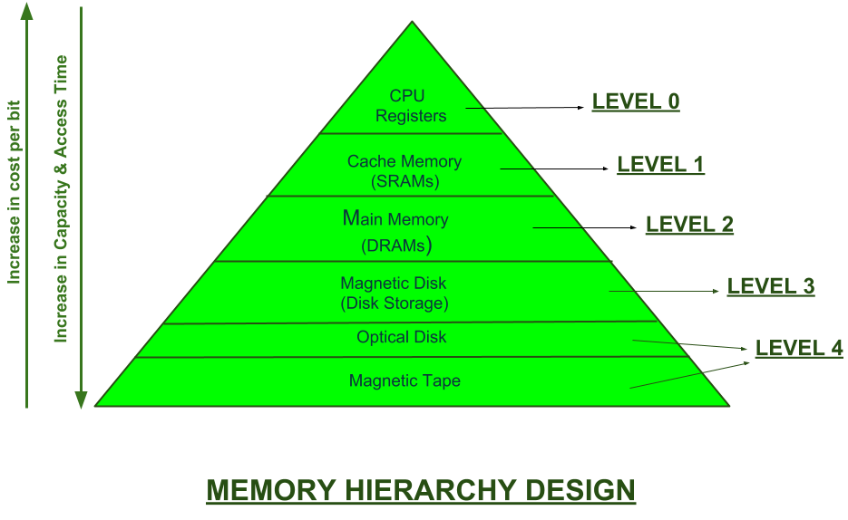
This Memory Hierarchy Design is divided into 2 main types:
- External Memory or Secondary Memory –
Comprising of Magnetic Disk, Optical Disk, Magnetic Tape i.e. peripheral storage devices which are accessible by the processor via I/O Module. - Internal Memory or Primary Memory –
Comprising of Main Memory, Cache Memory & CPU registers. This is directly accessible by the processor.
We can infer the following characteristics of Memory Hierarchy Design from above figure:
- Capacity:
It is the global volume of information the memory can store. As we move from top to bottom in the Hierarchy, the capacity increases. - Access Time:
It is the time interval between the read/write request and the availability of the data. As we move from top to bottom in the Hierarchy, the access time increases. - Performance:
Earlier when the computer system was designed without Memory Hierarchy design, the speed gap increases between the CPU registers and Main Memory due to large difference in access time. This results in lower performance of the system and thus, enhancement was required. This enhancement was made in the form of Memory Hierarchy Design because of which the performance of the system increases. One of the most significant ways to increase system performance is minimizing how far down the memory hierarchy one has to go to manipulate data. - Cost per bit:
As we move from bottom to top in the Hierarchy, the cost per bit increases i.e. Internal Memory is costlier than External Memory
Microprocessors perform calculations at tremendous speeds, but this is
only useful if the needed data for those calculations is available at sim-
ilar speeds. If the processor is the engine of your computer, then data
would be its fuel, and the faster the processor runs, the more quickly it
must be supplied with new data to keep performing useful work. As
processor performance has improved, the total capacity of data they are
asked to handle has increased. Modern computers can store the text of
thousands of books, but it is also critical to provide the processor with
the right piece of data at the right time. Without low latency to access the
data the processor is like a speed-reader in a vast library, wandering for
hours trying to find the right page of a particular book.
Ideally, the data store of a processor should have extremely large
capacity and extremely small latency, so that any piece of a vast amount
of data could be very quickly accessed for calculation. In reality, this isn’t
practical because the low latency means of storage are also the most
expensive. To provide the illusion of a large-capacity, low-latency
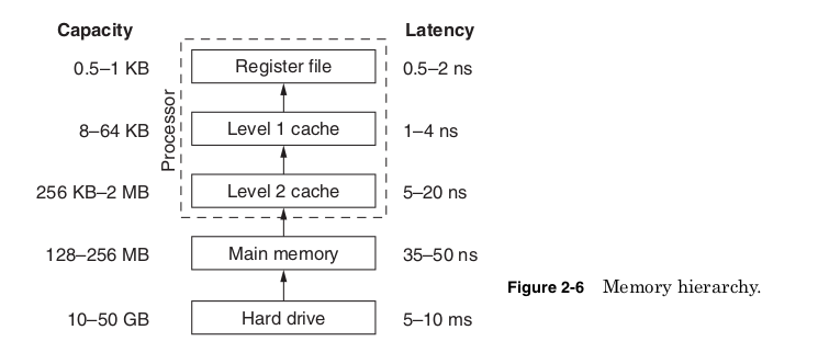
memory store, modern computers use a memory hierarchy (Fig. 2-6).
This uses progressively larger but longer latency memory stores to hold
all the data, which may eventually be needed while providing quick
access to the portion of the data currently being used.
The top of the memory hierarchy, the register file, typically contains
between 64 and 256 values that are the only numbers on which the
processor performs calculations. Before any two numbers are added,
multiplied, compared, or used in any calculation, they will first be loaded
into registers. The register file is implemented as a section of transis-
tors at the heart of the microprocessor die. Its small size and physical
location directly next to the portion of the die performing calculations
are what make its very low latencies possible. The effective cost of this
die area is extremely high because increasing the capacity of the regis-
ter file will push the other parts of the die farther apart, possibly lim-
iting the maximum processor frequency. Also the latency of the register
file will increase if its capacity is increased.

Making any memory store larger will always increase its access time.
So the register file is typically kept small to allow it to provide laten-
cies of only a few processor cycles; but operating at billions of calcula-
tions per second, it won’t be long before the processor will need a piece
of data not in the register file. The first place the processor looks next
for data is called cache memory.
Cache memory is high-speed memory built into the processor die. It
has higher capacity than the register file but a longer latency. Cache
memories reduce the effective memory latency by storing data that has
recently been used. If the processor accesses a particular memory loca-
tion while running a program, it is likely to access it more than once.
Nearby memory locations are also likely to be needed.
By loading and storing memory values and their neighboring locations
as they are accessed, cache memory will often contain the data the
processor needs. If the needed data is not found in the cache, it will have
to be retrieved from the next level of the memory hierarchy, the com-
puter’s main memory. The percentage of time the needed data is found
when the cache is accessed is called the hit rate. A larger cache will pro-
vide a higher hit rate but will also take up more die area, increasing the
processor cost. In addition, the larger the cache capacity, the longer its
latency will be. Table 2-10 shows some of the trade-offs in designing
cache memory.
All the examples in Table 2-10 assume an average access time to
main memory of 50 processor cycles. The first column shows that a
processor with no cache will always have to go to main memory and
therefore has an average access time of 50 cycles. The next column
shows a 4-kB cache giving a hit rate of 65 percent and a latency of 4 cycles.
For each memory access, there is a 65 percent chance the data will be
found in the cache (a cache hit) and made available after 4 cycles.

If the data is not found (a cache miss), it will be retrieved from main
memory after 50 cycles. This gives an average access time of 21.5 cycles.
Increasing the size of the cache increases the hit rate and the latency
of the cache. For this example, the average access time is improved by
using a 32-kB cache but begins to increase as the cache size is increased
to 128 kB. At the larger cache sizes the improvement in hit rate is not
enough to offset the increased latency.
The last column of the table shows the most common solution to this
trade-off, a multilevel cache. Imagine a processor with a 4-kB level 1
cache and a 128-kB level 2 cache. The level 1 cache is always accessed
first. It provides fast access even though its hit rate is not especially
good. Only after a miss in the level 1 cache is the level 2 cache accessed.
It provides better hit rate and its higher latency is acceptable because
it is accessed much less often than the level 1 cache. Only after misses
in both levels of cache is main memory accessed. For this example, the
two-level cache gives the lowest overall average access time, and all
modern high performance processors incorporate at least two levels
of cache memory including the Intel Pentium II/III/4 and AMD Athlon/
Duron/Opteron.
If a needed piece of data is not found in any of the levels of cache or
in main memory, then it must be retrieved from the hard drive. The hard
drive is critical of course because it provides permanent storage that is
retained even when the computer is powered down, but when the com-
puter is running the hard drive acts as an extension of the memory
hierarchy. Main memory and the hard drive are treated as being made
up of fixed-size “pages” of data by the operating system and micro-
processor. At any given moment a page of data might be in main memory
or might be on the hard drive. This mechanism is called virtual memory
since it creates the illusion of the hard drive acting as memory.
For each memory access, the processor checks an array of values
stored on the die showing where that particular piece of data is being
stored. If it is currently on the hard drive, the processor signals a page
fault. This interrupts the program currently being run and causes a por-
tion of the operating system program to run in its place. This handler
program writes one page of data in main memory back to the hard drive
and then copies the needed page from the hard drive into main memory.
The program that caused the page fault then continues from the point
it left off.
Through this slight of hand the processor and operating system
together make it appear that the needed information was in memory all
the time. This is the same kind of swapping that goes on between main
memory and the processor cache. The only difference is that the operating
system and processor together control swapping from the hard drive to
memory, whereas the processor alone controls swapping between memory
and the cache. All of these levels of storage working together provide the
illusion of a memory with the capacity of your hard drive but an effective
latency that is dramatically faster.
We can picture a processor using the memory hierarchy the way a man
working in an office might use filing system. The registers are like a
single line on a sheet of paper in the middle of his desk. At any given
moment he is only reading or writing just one line on this one piece of
paper. The whole sheet of paper acts like the level 1 cache, containing
other lines that he has just read or is about to read. The rest of his desk
acts like the level 2 cache holding other sheets of paper that he has
worked on recently, and a large table next to his desk might represent
main memory. They each hold progressively more information but take
longer to access. His filing cabinet acts like a hard drive storing vast
amounts of information but taking more time to find anything in it.
Our imaginary worker is able to work efficiently because most of time
after he reads one line on a page, he also reads the next line. When finished
with one page, most of the time the next page he needs is already out
on his desk or table. Only occasionally does he need to pull new pages
from the filing cabinet and file away pages he has changed. Of course,
in this imaginary office, after hours when the business is “powered
down,” janitors come and throw away any papers left on his desk or
table. Only results that he has filed in his cabinet, like saving to the hard
drive, will be kept. In fact, these janitors are somewhat unreliable and
will occasionally come around unannounced in the middle of the day to
throw away any lose papers they find. Our worker would be wise to file
results a few times during the day just in case.
The effective latency of the memory hierarchy is ultimately deter-
mined not only by the capacity and latency of each level of the hier-
archy, but also by the way each program accesses data. Programs that
operate on small data sets have better hit rates and lower average
access times than programs that operate on very large data sets.
Microprocessors designed for computer servers often add more or larger
levels of cache because servers often operate on much more data than
typical users require. Computer performance is also hurt by excessive
page faults caused by having insufficient main memory. A balanced
memory hierarchy from top to bottom is a critical part of any computer.
The need for memory hierarchy has arisen because memory per-
formance has not increased as quickly as processor performance. In
DRAMs, transistor scaling has been used instead to provide more
memory capacity. This allows for larger more complex programs but
limits the improvements in memory frequency. There is no real advantage
to running the bus that transfers data from memory to the processor at a
higher frequency than the memory supports.

Figure 2-7 shows how processor frequency has scaled over time com-
pared to the processor bus transfer rate. In the 1980s, processor fre-
quency and the bus transfer rate were the same. The processor could
receive new data every cycle. In the early 2000s, it was common to have
transfer rates of only one-fifth the processor clock rate. To compensate
for the still increasing gap between processor and memory perform-
ance, processors have added steadily more cache memory and more
levels of memory hierarchy.
The first cache memories used in PCs were high-speed SRAM chips
added to motherboards in the mid-1980s (Fig. 2-8). Latency for these
chips was lower than main memory because they used SRAM cells
instead of DRAM and because the processor could access them directly
without going through the chipset. For the same capacity, these SRAM
chips could be as much as 30 times more expensive, so there was no hope
of replacing the DRAM chips used for main memory, but a small SRAM
cache built into the motherboard did improve performance.
As transistor scaling continued, it became possible to add a level 1
cache to the processor die itself without making the die size unreason-
ably large. Eventually this level 1 cache was split into two caches, one
for holding instructions and one for holding data. This improved

performance mainly by allowing the processor to access new instructions
and data simultaneously.
In the mid-1990s, the memory hierarchy reached an awkward point.
Transistor scaling had increased processor frequencies enough that
level 2 cache on the motherboard was significantly slower than caches
built into the die. However, transistors were still large enough that an
on-die level 2 cache would make the chips too large to be economically
produced. A compromise was reached in “slot” packaging. These large
plastic cartridges contained a small printed circuit board made with the
same process as motherboards. On this circuit board were placed the
processor and SRAM chips forming the level 2 cache. By being placed
in the same package the SRAM chips could be accessed at or near the
processor frequency. Manufacturing the dies separately allowed production
costs to be controlled.
By the late 1990s, continued shrinking of transistors allowed the
in-package level 2 cache to be moved on die, and slot packaging was
phased out. In the early 2000s, some processors now include three levels
of on-die cache. It seems likely that the gap between memory and proces-
sor frequency will continue to grow, requiring still more levels of cache
memory, and the die area of future processors may be dominated by the
cache memory and not the processor logic.
he number of levels in the memory hierarchy and the performance at each level has increased over time. The type of memory or storage components also change historically For example, the memory hierarchy of an Intel Haswell Mobile [7] processor circa 2013 is:
- Processor registers – the fastest possible access (usually 1 CPU cycle). A few thousand bytes in size
- Cache
- Level 0 (L0) Micro operations cache – 6 KiB in size
- Level 1 (L1) Instruction cache – 128 KiB in size
- Level 1 (L1) Data cache – 128 KiB in size. Best access speed is around 700 GiB/second
- Level 2 (L2) Instruction and data (shared) – 1 MiB in size. Best access speed is around 200 GiB/second
- Level 3 (L3) Shared cache – 6 MiB in size. Best access speed is around 100 GB/second
- Level 4 (L4) Shared cache – 128 MiB in size. Best access speed is around 40 GB/second
- Main memory (Primary storage) – Gigabytes in size. Best access speed is around 10 GB/second.In the case of a NUMA machine, access times may not be uniform
- Disk storage (Secondary storage) – Terabytes in size. As of 2017, best access speed is from a consumer solid state drive is about 2000 MB/second
- Nearline storage (Tertiary storage) – Up to exabytes in size. As of 2013, best access speed is about 160 MB/second
- Offline storage
The lower levels of the hierarchy – from disks downwards – are also known as tiered storage. The formal distinction between online, nearline, and offline storage is:
- Online storage is immediately available for I/O.
- Nearline storage is not immediately available, but can be made online quickly without human intervention.
- Offline storage is not immediately available, and requires some human intervention to bring online.
For example, always-on spinning disks are online, while spinning disks that spin-down, such as massive array of idle disk (MAID), are nearline. Removable media such as tape cartridges that can be automatically loaded, as in a tape library, are nearline, while cartridges that must be manually loaded are offline.
Most modern CPUs are so fast that for most program workloads, the bottleneck is the locality of reference of memory accesses and the efficiency of the caching and memory transfer between different levels of the hierarchy[citation needed]. As a result, the CPU spends much of its time idling, waiting for memory I/O to complete. This is sometimes called the space cost, as a larger memory object is more likely to overflow a small/fast level and require use of a larger/slower level. The resulting load on memory use is known as pressure (respectively register pressure, cache pressure, and (main) memory pressure). Terms for data being missing from a higher level and needing to be fetched from a lower level are, respectively: register spilling (due to register pressure: register to cache), cache miss (cache to main memory), and (hard) page fault (main memory to disk).
Modern programming languages mainly assume two levels of memory, main memory and disk storage, though in assembly language and inline assemblers in languages such as C, registers can be directly accessed. Taking optimal advantage of the memory hierarchy requires the cooperation of programmers, hardware, and compilers (as well as underlying support from the operating system):
- Programmers are responsible for moving data between disk and memory through file I/O.
- Hardware is responsible for moving data between memory and caches.
- Optimizing compilers are responsible for generating code that, when executed, will cause the hardware to use caches and registers efficiently.
Many programmers assume one level of memory. This works fine until the application hits a performance wall. Then the memory hierarchy will be assessed during code refactoring.
Conclusion
When looking at a computer, the most noticeable features are things like
the monitor, keyboard, mouse, and disk drives, but these are all simply
input and output devices, ways of getting information into or out of the com-
puter. For computer performance or compatibility, the components that are
most important are those that are the least visible, the microprocessor,
chipset, and motherboard. These components and how well they com-
municate with the rest of the system will determine the performance of
the product, and it is the overall performance of the product and not the
processor that matters. To create a product with the desired performance,
we must design the processor to work well with the other components.
The way a processor will communicate must be considered before
starting any design. As processor performance has increased, the com-
ponents that move data into and out of the processor have become
increasingly important. An increasing variety of available components
and bus standards have made the flexibility of separate chipsets more
attractive, but at the same time the need for lower latencies encourages
building more communication logic directly into the processor. The right
trade-off will vary greatly, especially since today processors may go into
many products very different from a traditional computer.
Handheld devices, entertainment electronics, or other products with
embedded processors may have very different performance requirements
and components than typical PCs, but they still must support buses for
communication and deal with rapidly changing standards. The basic
need to support data into and out of a processor, nonvolatile storage, and
peripherals is the same for a MP3 player or a supercomputer. Keeping
in mind these other components that will shape the final product, we are
ready to begin planning the design of the microprocessor.
Key Concept and term

