by Dr. Jaydeep T. Vagh
Overview
This chapter presents an overview of the entire microprocessor design
flow and discusses design targets including processor roadmaps, design
time, and product cost.
Objectives
Upon completion of this chapter, the reader will be able to:
- Explain the overall microprocessor design flow.
- Understand the different processor market segments and their
requirements. - Describe the difference between lead designs, proliferations, and
compactions. - Describe how a single processor design can grow into a family of
products. - Understand the common job positions on a processor design team.
- Calculate die cost, packaging cost, and overall processor cost.
- Describe how die size and defect density impacts processor cost.
Intro
Transistor scaling and growing transistor budgets have allowed micro-
processor performance to increase at a dramatic rate, but they have
also increased the effort of microprocessor design. As more functionality
is added to the processor, there is more potential for logic errors. As clock
rates increase, circuit design requires more detailed simulations. The
production of new fabrication generations is inevitably more complex
than previous generations. Because of the short lifetime of most micro-
processors in the marketplace, all of this must happen under the pres-
sure of an unforgiving schedule. The general steps in processor design
are shown in Fig. 3-1.
A microprocessor, like any product, must begin with a plan, and the
plan must include not only a concept of what the product will be, but
also how it will be created. The concept would need to include the type
of applications to be run as well as goals for performance, power, and
cost. The planning will include estimates of design time, the size of the
design team, and the selection of a general design methodology.
Defining the architecture involves choosing what instructions
the processor will be able to execute and how these instructions will
be encoded. This will determine whether already existing software can
be used or whether software will need to be modified or completely rewrit-
ten. Because it determines the available software base, the choice of
architecture has a huge influence on what applications ultimately run on
the processor. In addition, the performance and capabilities of the proces-
sor are in part determined by the instruction set. Design planning and
defining an architecture is the design specification stage of the project,
since completing these steps allows the design implementation to begin.
Although the architecture of a processor determines the instructions
that can be executed, the microarchitecture determines the way in which

they are executed. This means that architectural changes are visible to
the programmer as new instructions, but microarchitectural changes
are transparent to the programmer. The microarchitecture defines the
different functional units on the processor as well as the interactions and
division of work between them. This will determine the performance per
clock cycle and will have a strong effect on what clock rate is ultimately
achievable.
Logic design breaks the microarchitecture down into steps small
enough to prove that the processor will have the correct logical behav-
ior. To do this a computer simulation of the processor’s behavior is writ-
ten in a register transfer language (RTL). RTL languages, such as Verilog
and VHDL, are high-level programming languages created specifically
to simulate computer hardware. It is ironic that we could not hope to
design modern microprocessors without high-speed microprocessors to
simulate the design. The microarchitecture and logic design together
make up the behavioral design of the project.
Circuit design creates a transistor implementation of the logic spec-
ified by the RTL. The primary concerns at this step are simulating the
clock frequency and power of the design. This is the first step where the
real world behavior of transistors must be considered as well as how that
behavior changes with each fabrication generation.
Layout determines the positioning of the different layers of material
that make up the transistors and wires of the circuit design. The pri-
mary focus is on drawing the needed circuit in the smallest area that
still can be manufactured. Layout also has a large impact on the fre-
quency and reliability of the circuit. Together circuit design and layout
specify the physical design of the processor.
The completion of the physical design is called tapeout. In the past
upon completion of the layout, all the needed layers were copied onto a
magnetic tape to be sent to the fab, so manufacturing could begin. The
day the tape went to the fab was tapeout. Today the data is simply
copied over a computer network, but the term tapeout is still used to
describe the completion of the physical design.
After tapeout the first actual prototype chips are manufactured.
Another major milestone in the design of any processor is first silicon,
the day the first chips arrive from the fab. Until this day the entire
design exists as only computer simulations. Inevitably reality is not
exactly the same as the simulations predicted. Silicon debug is the
process of identifying bugs in prototype chips. Design changes are made
to correct any problems as well as improving performance, and new
prototypes are created. This continues until the design is fit to be sold,
and the product is released into the market.
After product release the production of the design begins in earnest.
However, it is common for the design to continue to be modified even
after sales begin. Changes are made to improve performance or reduce
the number of defects. The debugging of initial prototypes and movement
into volume production is called the silicon ramp.
Throughout the design flow, validation works to make sure each
step is performed correctly and is compatible with the steps before and
after. For a large from scratch processor design, the entire design flow
might take between 3 and 5 years using anywhere from 200 to 1000
people. Eventually production will reach a peak and then be gradually
phased out as the processor is replaced by newer designs.
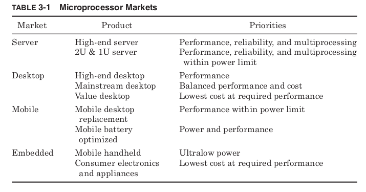
Processor Roadmaps

The design of any microprocessor has to start with an idea of what type
of product will use the processor. In the past, designs for desktop com-
puters went through minor modifications to try and make them suitable
for use in other products, but today many processors are never intended
for a desktop PC. The major markets for processors are divided into
those for computer servers, desktops, mobile products, and embedded
applications.
Servers and workstations are the most expensive products and there-
fore can afford to use the most expensive microprocessors. Performance
and reliability are the primary drivers with cost being less important.
Most server processors come with built-in multiprocessor support to
easily allow the construction of computers using more than one proces-
sor. To be able to operate on very large data sets, processors designed
for this market tend to use very large caches. The caches may include
parity bits or Error Correcting Codes (ECC) to improve reliability.
Scientific applications also make floating-point performance much more
critical than mainstream usage.
The high end of the server market tends to tolerate high power levels,
but the demand for “server farms,” which provide very large amounts
of computing power in a very small physical space, has led to the cre-
ation of low power servers. These “blade” servers are designed to be
loaded into racks one next to the other. Standard sizes are 2U (3.5-in
thick) and 1U (1.75-in thick). In such narrow dimensions, there isn’t
room for a large cooling system, and processors must be designed to con-
trol the amount of heat they generate. The high profit margins of server
processors give these products a much larger influence on the processor
industry than their volumes would suggest.
Desktop computers typically have a single user and must limit their
price to make this financially practical. The desktop market has further
differentiated to include high performance, mainstream, and value
processors. The high-end desktop computers may use processors with per-
formance approaching that of server processors, and prices approaching


them as well. These designs will push die size and power levels to the
limits of what the desktop market will bear. The mainstream desktop
market tries to balance cost and performance, and these processor
designs must weigh each performance enhancement against the increase
in cost or power. Value processors are targeted at low-cost desktop sys-
tems, providing less performance but at dramatically lower prices. These
designs typically start with a hard cost target and try to provide the most
performance possible while keeping cost the priority.
Until recently mobile processors were simply desktop processors repack-
aged and run at lower frequencies and voltages to reduce power, but the
extremely rapid growth of the mobile computer market has led to many
designs created specifically for mobile applications. Some of these are
designed for “desktop replacement” notebook computers. These notebooks
are expected to provide the same level of performance as a desktop com-
puter, but sacrifice on battery life. They provide portability but need to
be plugged in most of the time. These processors must have low enough
power to be successfully cooled in a notebook case but try to provide the
same performance as desktop processors. Other power-optimized proces-
sors are intended for mobile computers that will typically be run off bat-
teries. These designs will start with a hard power target and try to provide
the most performance within their power budget.
Embedded processors are used inside products other than computers.
Mobile handheld electronics such as Personal Digital Assistants (PDAs),
MP3 players, and cell phones require ultralow power processors, which need
no special cooling. The lowest cost embedded processors are used in a huge
variety of products from microwaves to washing machines. Many of these
products need very little performance and choose a processor based mainly
on cost. Microprocessor markets are summarized in Table 3-1.
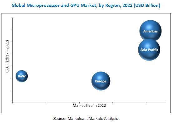
Global Microprocessor Market Will Reach USD 8,894 Million By 2025: Zion Market Research
Global Microprocessor Market: Architecture Analysis
- X86
- ARM
- MIPS
- Power
- SPARC
Global Microprocessor Market: Type Analysis
- Integrated Graphics
- Discrete Graphics
- Video Graphics Adapter
- Analog-To-Digital and Digital-To-Analog Converter
- Peripheral Component Interconnects Bus
- Universal Serial Bus
- Direct Memory Access Controller
- Others
Global Microprocessor Market: Application Analysis
- Smartphones
- Personal Computers
- Servers
- Tablets
- Embedded Devices
- Others
Global Microprocessor Market: Vertical Analysis
- Consumer Electronics
- Server
- Automotive
- Banking, Financial Services, and Insurance (BFSI)
- Aerospace and Defense
- Medical
- Industrial
Global Microprocessor Market: Regional Analysis
- North America
- The U.S.
- Europe
- UK
- France
- Germany
- Asia Pacific
- China
- Japan
- India
- Latin America
- Brazil
- The Middle East and Africa
In addition to targets for performance, cost, and power, software and
hardware support are also critical. Ultimately all a processor can do is
run software, so a new design must be able to run an existing software
base or plan for the impact of creating new software. The type of soft-
ware applications being used changes the performance and capabilities
needed to be successful in a particular product market.
The hardware support is determined by the processor bus standard
and chipset support. This will determine the type of memory, graphics
cards, and other peripherals that can be used. More than one processor
project has failed, not because of poor performance or cost, but because
it did not have a chipset that supported the memory type or peripherals
in demand for its product type.
For a large company that produces many different processors, how
these different projects will compete with each other must also be con-
sidered. Some type of product roadmap that targets different potential
markets with different projects must be created.
Figure 3-2 shows the Intel roadmap for desktop processors from 1999
to 2003. Each processor has a project name used before completion of the
design as well as a marketing name under which it is sold. To maintain
name recognition, it is common for different generations of processor
design to be sold under the same marketing name. The process genera-
tion will determine the transistor budget within a given die size as well
as the maximum possible frequency. The frequency range and cache size
of the processors give an indication of performance, and the die size gives
a sense of relative cost. The Front-Side Bus (FSB) transfer rate determines
how quickly information moves into or out of the processor. This will
influence performance and affect the choice of motherboard and memory.
Figure 3-2 begins with the Katmai project being sold as high-end
desktop in 1999. This processor was sold in a slot package that included
512 kB of level 2 cache in the package but not on the processor die. In
the same time frame, the Mendocino processor was being sold as a value
processor with 128 kB of cache. However, the Mendocino die was actu-
ally larger because this was the very first Intel project to integrate the
level 2 cache into the processor die. This is an important example of how
a larger die does not always mean a higher product cost. By including
the cache on the processor die, separate SRAM chips and a multichip
package were no longer needed. Overall product cost can be reduced even
when die costs increase.
As the next generation Coppermine design appeared, Katmai was
pushed from the high end. Later, Coppermine was replaced by the
Willamette design that was sold as the first Pentium 4. This design
enabled much higher frequencies but also used a much larger die. It
became much more profitable when converted to the 130-nm process
generation by the Northwood design. By the end of 2002, the Northwood
design was being sold in all the desktop markets. At the end of 2003, the
Gallatin project added 2 MB of level 3 cache to the Northwood design
and was sold as the Pentium 4 Extreme Edition.
It is common for identical processor die to be sold into different market
segments. Fuses are set by the manufacturer to fix the processor fre-
quency and bus speed. Parts of the cache memory and special instruc-
tion extensions may be enabled or disabled. The same die may also be
sold in different types of packages. In these ways, the manufacturer cre-
ates varying levels of performance to be sold at different prices.
Figure 3-2 shows in 2003 the same Northwood design being sold as a
Pentium 4 in the high-end and mainstream desktop markets as well as
a Celeron in the value market. The die in the Celeron product is iden-
tical to die used in the Pentium 4 but set to run at lower frequency, a
lower bus speed, and with half of the cache disabled. It would be possi-
ble to have a separate design with only half the cache that would have a
smaller die size and cost less to produce. However, this would require
careful planning for future demand to make sure enough of each type
of design was available. It is far simpler to produce a single design and
then set fuses to enable or disable features as needed.
It can seem unfair that the manufacturer is intentionally “crippling”
their value products. The die has a full-sized cache, but the customer
isn’t allowed to use it. The manufacturing cost of the product would be
no different if half the cache weren’t disabled. The best parallel to this
situation might be the cable TV business. Cable companies typical
charge more for access to premium channels even though their costs do
not change at all based on what the customer is watching. Doing this
allows different customers to pay varying amounts depending on what
features they are using. The alternative would be to charge everyone the
same, which would let those who would pay for premium features have
a discount but force everyone else to pay for features they don’t really
need. By charging different rates, the customer is given more choices and
able to pay for only what they want.
Repackaging and partially disabling processor designs allow for more
consumer choice in the same way. Some customers may not need the full
bus speed or full cache size. By creating products with these features
disabled a wider range of prices are offered and the customer has more
options. The goal is not to deny good products to customers but to charge
them for only what they need.
Smaller companies with fewer products may target only some mar-
kets and may not be as concerned about positioning their own products
relative to each other, but they must still create a roadmap to plan the
positioning of their products relative to competitors. Once a target
market and features have been identified, design planning addresses
how the design is to be made.
Design Types and Design Time
How much of a previous design is reused is the biggest factor affecting
processor design time. Most processor designs borrow heavily from ear-
lier designs, and we can classify different types of projects based on
what parts of the design are new (Table 3-2).
Designs that start from scratch are called lead designs. They offer
the most potential for improved performance and added features by
allowing the design team to create a new design from the ground up. Of
course, they also carry the most risk because of the uncertainty of
creating an all-new design. It is extremely difficult to predict how long
lead designs will take to complete as well as their performance and die
size when completed. Because of these risks, lead designs are relatively
rare.
Most processor designs are compactions or variations. Compactions
take a completed design and move it to a new manufacturing process
while making few or no changes in the logic. The new process allows an
old design to be manufactured at less cost and may enable higher fre-
quencies or lower power. Variations add some significant logical features
to a design but do not change the manufacturing process. Added features
might be more cache, new instructions, or performance enhancements.
Proliferations change the manufacturing process and make significant
logical changes.
The simplest way of creating a new processor product is to repack-
age an existing design. A new package can reduce costs for the value
market or enable a processor to be used in mobile applications where it
couldn’t physically fit before. In these cases, the only design work is
revalidating the design in its new package and platform.
Intel’s Pentium 4 was a lead design that reused almost nothing from
previous generations. Its schedule was described at the 2001 Design
Automation Conference as approximately 6 months to create a design
specification, 12 months of behavioral design, 18 months of physical


design, and 12 months of silicon debug, for a total of 4 years from design
plan to shipping. 1 A compaction or variation design might cut this time
in half by reusing significant portions of earlier designs. A proliferation
would fall somewhere in between a lead design and a compaction. A
repackaging skips all the design steps except for silicon debug, which
presumably will go more quickly for a design already validated in a
different platform. See Figure 3-3.
Of course, the design times shown in Fig. 3-3 are just approximations.
The actual time required for a design will also depend on the overall design
complexity, the level of automation being used, and the size of the design
team. Productivity is greatly improved if instead of working with individual
logic gates, engineers are using larger predesigned blocks in constructing
their design. The International Technology Roadmap for Semiconductors
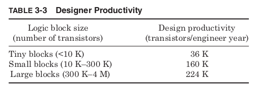
(ITRS) gives design productivity targets based on the size of the logic
blocks being used to build the design. 2 Assuming an average of four tran-
sistors per logic gate gives the productivity targets shown in Table 3-3.
Constructing a design out of pieces containing hundreds of thousands
or millions of transistors implies that someone has already designed
these pieces, but standard libraries of basic logical components are
created for a given manufacturing generation and then assembled into
many different designs. Smaller fabless companies license the use of
these libraries from manufacturers that sell their own spare manufac-
turing capacity. The recent move toward dual core processors is driven
in part by the increased productivity of duplicating entire processor cores
for more performance rather than designing ever-more complicated cores.
The size of the design team needed will be determined both by the type
of design and the designer productivity with team sizes anywhere from
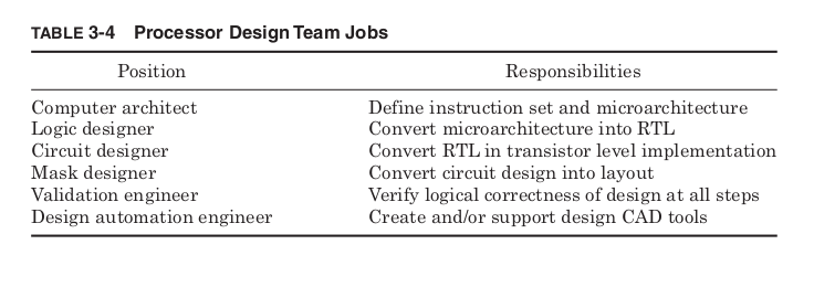
less than 50 to more than 1000. The typical types of positions are shown
in Table 3-4.
The larger the design team, the more additional personnel will be
needed to manage and organize the team, growing the team size even
more. For design teams of hundreds of people, the human issues of clear
communication, responsibility, and organization become just as impor-
tant as any of the technical issues of design.
The headcount of a processor project typically grows steadily until
tapeout when the layout is first sent to be fabricated. The needed head-
count drops rapidly after this, but silicon debug and beginning of produc-
tion may still require large numbers of designers working on refinements
for as much as a year after the initial design is completed. One of the most
important challenges facing future processor designs is how to enhance pro-
ductivity to prevent ever-larger design teams even as transistors budgets
continue to grow.
The design team and manpower required for lead designs are so high
that they are relatively rare. As a result, the vast majority of processor
designs are derived from earlier designs, and a great deal can be learned
about a design by looking at its family tree. Because different proces-
sor designs are often sold under a common marketing name, tracing the
evolution of designs requires deciphering the design project names. For
design projects that last years, it is necessary to have a name long before
the environment into which the processor will eventually be sold is
known for certain. Therefore, the project name is chosen long before the
product name and usually chosen with the simple goal of avoiding trade-
mark infringement.
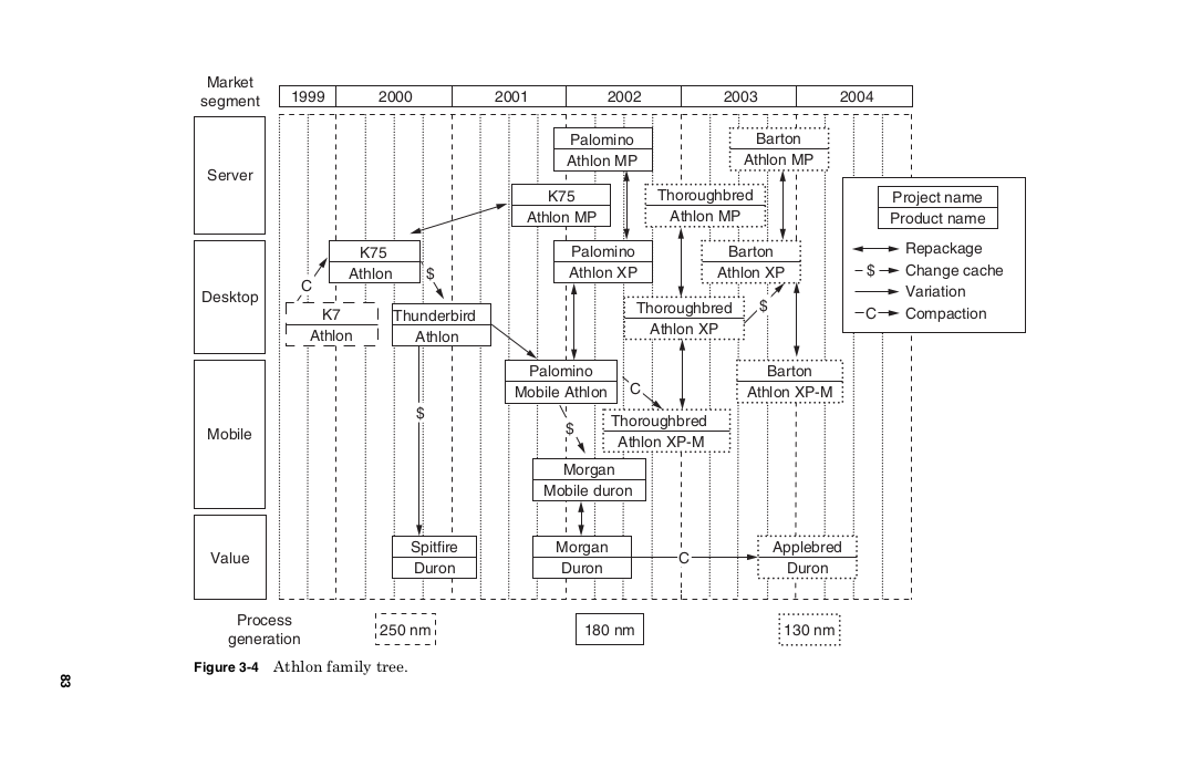
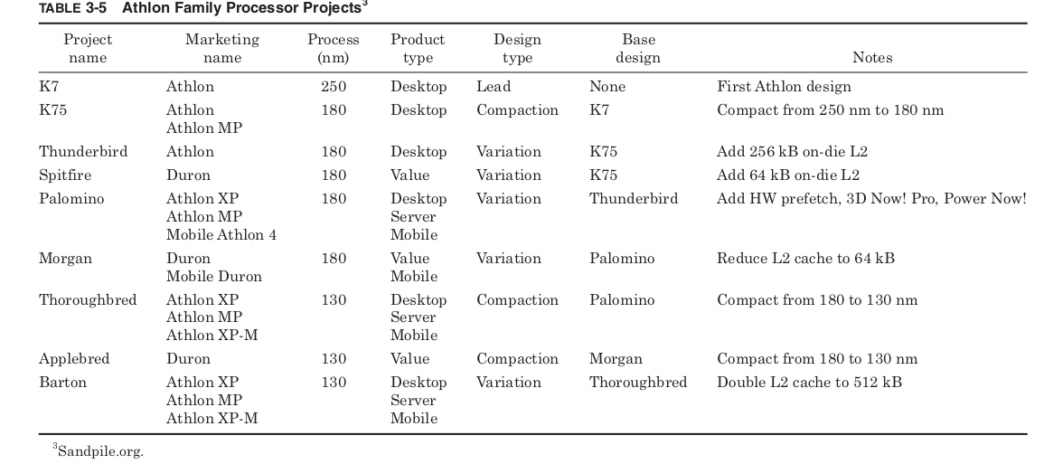
Figure 3-4 shows the derivation of the AMD Athlon ® designs. Each box
shows the project name and marketing name of a processor design with
the left edge showing when it was first sold.
The original Athlon design project was called the K7 since it was AMD’s
seventh generation microarchitecture. The K7 used very little of previous
AMD designs and was fabricated in a 250-nm fabrication process. This
design was compacted to the 180-nm process by the K75 project, which
was sold as both a desktop product, using the name Athlon, and a server
product with multiprocessing enabled, using the name Athlon MP. Both
the K7 and K75 used slot packaging with separate SRAM chips in the
same package acting as a level 2 cache.
The Thunderbird project added the level 2 cache to the processor die
eventually allowing the slot packaging to be abandoned. A low cost ver-
sion with a smaller level 2 cache, called Spitfire, was also created. To
make its marketing as a value product clear, the Spitfire design was
given a new marketing name, Duron ® .
The Palomino design added a number of enhancements. A hardware
prefetch mechanism was added to try and anticipate what data would
be used next and pull it into the cache before it was needed. A number
of new processor instructions were added to support multimedia oper-
ations. Together these instructions were called 3D Now! ® Professional.
Finally a mechanism was included to allow the processor to dynamically
scale its power depending on the amount of performance required by the
current application. This feature was marketed as Power Now! ® .
The Palomino was first sold as a mobile product but was quickly
repackaged for the desktop and sold as the first Athlon XP. It was also
marketed as the Athlon MP as a server processor. The Morgan project
removed three-fourths of the level 2 cache from the Palomino design to
create a value product sold as a Duron and Mobile Duron.
The Thoroughbred and Applebred projects were both compactions
that converted the Palomino and Morgan designs from the 180-nm gen-
eration to 130 nm. Finally, the Barton project doubled the size of the
Thoroughbred cache. The Athlon 64 chips that followed were based on
a new lead design, so Barton marked the end of the family of designs
based upon the original Athlon. See Table 3-5.
Because from scratch designs are only rarely attempted, for most
processor designs the most important design decision is choosing the pre-
vious design on which the new product will be based.
Product Cost
A critical factor in the commercial success or failure of any product is
how much it costs to manufacture. For all processors, the manufactur-
ing process begins with blank silicon wafers. The wafers are cut from
cylindrical ingots and must be extremely pure and perfectly flat. Over
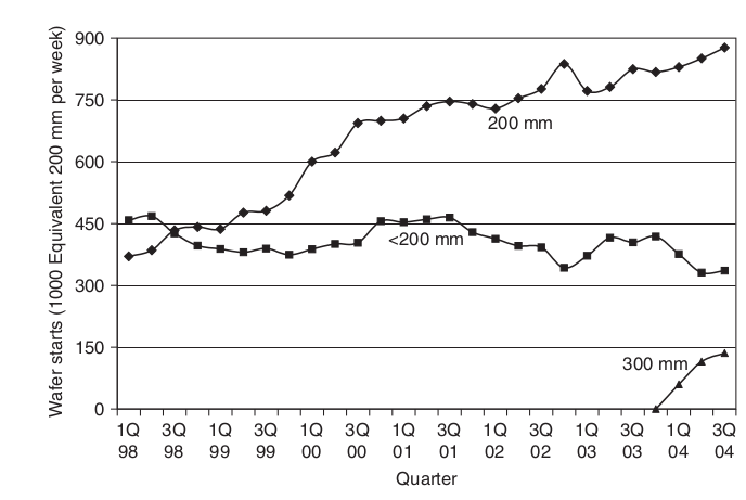
time the industry has moved to steadily larger wafers to allow more
chips to be made from each one. In 2004, the most common size used was
200-mm diameter wafers with the use of 300-mm wafers just begin-
ning (Fig. 3-5). Typical prices might be $20 for a 200-mm wafer and $200
4
for a 300-mm wafer. However, the cost of the raw silicon is typically only
a few percent of the final cost of a processor.
Much of the cost of making a processor goes into the fabrication facil-
ities that produce them. The consumable materials and labor costs of
operating the fab are significant, but they are often outweighed by the

cost of depreciation. These factories cost billions to build and become
obsolete in a few years. This means the depreciation in value of the fab
can be more than a million dollars every day. This cost must be covered
by the output of the fab but does not depend upon the number of wafers
processed. As a result, the biggest factor in determining the cost of pro-
cessing a wafer is typically the utilization of the factory. The more wafers
the fab produces, the lower the effective cost per wafer.
Balancing fab utilization is a tightrope all semiconductor companies
must walk. Without sufficient capacity to meet demand, companies will
lose market share to their competitors, but excess capacity increases the
cost per wafer and hurts profits. Because it takes years for a new fab to
be built and begin producing, construction plans must be based on pro-
jections of future demand that are uncertain. From 1999 to 2000,
demand grew steadily, leading to construction of many new facilities
(Fig. 3-6). Then unexpectedly low demand in 2001 left the entire semi-
conductor industry with excess capacity. Matching capacity to demand
is an important part of design planning for any semiconductor product.
The characteristics of the fab including utilization, material costs, and
labor will determine the cost of processing a wafer. In 2003, a typical
cost for processing a 200-mm wafer was $3000. 5 The size of the die will
determine the cost of an individual chip. The cost of processing a wafer does
not vary much with the number of die, so the smaller the die, the lesser
the cost per chip. The total number of die per wafer are estimated as:

The first term just divides the area of the wafer by the area of a single
die. The second term approximates the loss of rectangular die that do
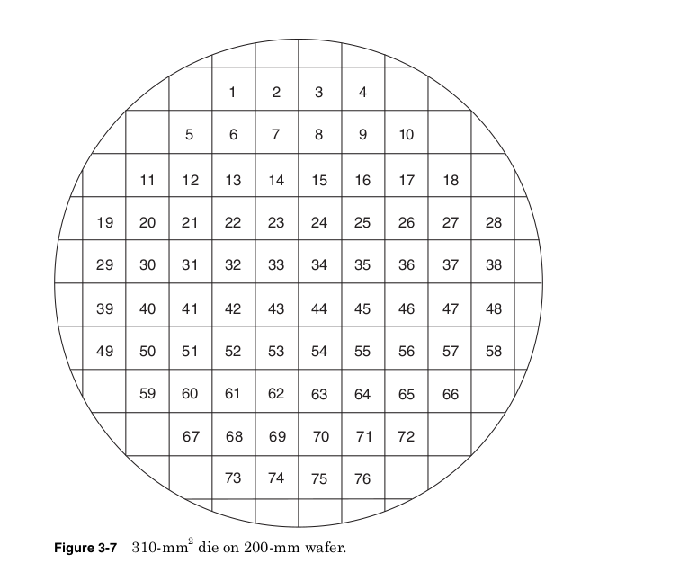
not entirely fit on the edge of the round wafer. The 2003 International
Technology Roadmap for Semiconductors (ITRS) suggests a target die
size of 140 mm 2 for a mainstream microprocessor and 310 mm 2 for a
server product. On 200-mm wafers, the equation above predicts the
mainstream die would give 186 die per wafer whereas the server die size
would allow for only 76 die per wafer. The 310-mm 2 die on 200-mm
wafer is shown in Fig. 3-7.
Unfortunately not all the die produced will function properly. In fact,
although it is something each factory strives for, in the long run 100 percent
yield will not give the highest profits. Reducing the on-die dimensions
allows more die per wafer and higher frequencies that can be sold at
higher prices. As a result, the best profits are achieved when the process
is always pushed to the point where at least some of the die fail. The
density of defects and complexity of the manufacturing process deter-
mine the die yield, the percentage of functional die. Assuming defects
are uniformly distributed across the wafer, the die yield is estimated as
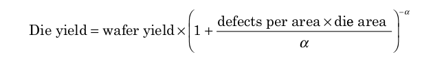
The wafer yield is the percentage of successfully processed wafers.
Inevitably the process flow fails altogether on some wafers preventing
any of the die from functioning, but wafer yields are often close to 100
percent. On good wafers the failure rate becomes a function of the fre-
quency of defects and the size of the die. In 2001, typical values for
defects per area were between 0.4 and 0.8 defects per square centimeter. 7
The value a is a measure of the complexity of the fabrication process with
more processing steps leading to a higher value. A reasonable estimate
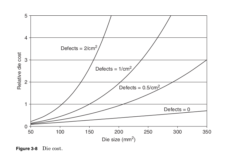
for modern CMOS processes is a = 4. 8 Assuming this value for a and
a 200-mm wafer, the calculation of the relative die cost for different
defect densities and die sizes.
Figure 3-8 shows how at very low defect densities, it is possible to pro-
duce very large die with only a linear increase in cost, but these die
quickly become extremely costly if defect densities are not well controlled.
At 0.5 defects per square centimeter and a = 4, the target mainstream
die size gives a yield of 50 percent while the server die yields only
25 percent.
Die are tested while still on the wafer to help identify failures as early
as possible. Only the die that pass this sort of test will be packaged. The
assembly of die into package and the materials of the package itself add
significantly to the cost of the product. Assembly and package costs
can be modeled as some base cost plus some incremental cost added per
package pin.
Package cost = base package cost + cost per pin × number of pins
The base package cost is determined primarily by the maximum power
density the package can dissipate. Low cost plastic packages might have
a base cost of only a few dollars and add only 0.5 cent per pin, but limit
the total power to less than 3 W. High-cost, high-performance packages
might allow power densities up to 100 W/cm 2 , but have base costs of $10
to $20 plus 1 to 2 cents per pin. 9 If high performance processor power
densities continue to rise, packaging could grow to be an even larger per-
centage of total product costs.
After packaging the die must again be tested. Tests before packaging
cannot screen out all possible defects, and new failures may have been
created during the assembly step. Packaged part testing identifies parts
to be discarded and the maximum functional frequency of good parts.
Testing typically takes less than 1 min, but every die must be tested and
the testing machines can cost hundreds of dollars per hour to operate.
All modern microprocessors add circuitry specifically to reduce test time
and keep test costs under control.

The final cost of the processor is the sum of the die, packaging, and
testing costs, divided by the yield of the packaged part testing.


Assuming typical values we can calculate the product cost of the ITRS
mainstream and server die sizes, as shown in Tables 3-6 and 3-7.
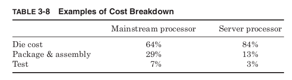
Calculating the percentage of different costs from these two examples
gives a sense of the typical contributions to overall processor cost.
Table 3-8 shows that the relative contributions to cost can be very dif-
ferent from one processor to another. Server products will tend to be
dominated by the cost of the die itself, but for mainstream processors
and especially value products, the cost of packaging, assembly, and test
cannot be overlooked. These added costs mean that design changes that
grow the die size do not always increase the total processor cost. Die
growth that allows for simpler packaging or testing can ultimately
reduce costs.
Whether a particular processor cost is reasonable depends of course
on the price of the final product the processor will be used in. In 2001,

the processor contributed approximately 20 percent to the cost of a typ-
ical $1000 PC. 10 If sold at $200 our desktop processor example costing
only $54 would show a large profit, but our server processor example at
$198 would give almost no profit. Producing a successful processor
requires understanding the products it will support.
Conclusion
Every processor begins as an idea. Design planning is the first step in
processor design and it can be the most important. Design planning
must consider the entire design flow from start to finish and answer sev-
eral important questions.

Errors or poor trade-offs in any of the later design steps can prevent
a processor from meeting its planned goals, but just as deadly to a proj-
ect is perfectly executing a poor plan or failing to plan at all.
The remaining chapters of this book follow the implementation of a
processor design plan through all the needed steps to reach manufac-
turing and ultimately ship to customers. Although in general these
steps do flow from one to the next, there are also activities going on in
parallel and setbacks that force earlier design steps to be redone. Even
planning itself will require some work from all the later design steps to
estimate what performance, power, and die area are possible. No single
design step is performed entirely in isolation. The easiest solution at one
step may create insurmountable problems for later steps in the design.
The real challenge of design is to understand enough of the steps before
and after your own specialty to make the right choices for the whole
design flow.