Analog signal processing is a type of signal processing conducted on continuousanalog signals by some analog means (as opposed to the discrete digital signal processing where the signal processing is carried out by a digital process). “Analog” indicates something that is mathematically represented as a set of continuous values. This differs from “digital” which uses a series of discrete quantities to represent signal. Analog values are typically represented as a voltage, electric current, or electric charge around components in the electronic devices. An error or noise affecting such physical quantities will result in a corresponding error in the signals represented by such physical quantities.
A system’s behavior can be mathematically modeled and is represented in the time domain as h(t) and in the frequency domain as H(s), where s is a complex number in the form of s=a+ib, or s=a+jb in electrical engineering terms (electrical engineers use “j” instead of “i” because current is represented by the variable i). Input signals are usually called x(t) or X(s) and output signals are usually called y(t) or Y(s).
Convolution
Convolution is the basic concept in signal processing that states an input signal can be combined with the system’s function to find the output signal. It is the integral of the product of two waveforms after one has reversed and shifted; the symbol for convolution is
That is the convolution integral and is used to find the convolution of a signal and a system; typically a = -∞ and b = +∞.
Consider two waveforms f and g. By calculating the convolution, we determine how much a reversed function g must be shifted along the x-axis to become identical to function f. The convolution function essentially reverses and slides function g along the axis, and calculates the integral of their (f and the reversed and shifted g) product for each possible amount of sliding. When the functions match, the value of (f*g) is maximized. This occurs because when positive areas (peaks) or negative areas (troughs) are multiplied, they contribute to the integral.
Fourier transform
The Fourier transform is a function that transforms a signal or system in the time domain into the frequency domain, but it only works for certain functions. The constraint on which systems or signals can be transformed by the Fourier Transform is that:
This is the Fourier transform integral:
Usually the Fourier transform integral isn’t used to determine the transform; instead, a table of transform pairs is used to find the Fourier transform of a signal or system. The inverse Fourier transform is used to go from frequency domain to time domain:
Each signal or system that can be transformed has a unique Fourier transform. There is only one time signal for any frequency signal, and vice versa
Laplace transform
The Laplace transform is a generalized Fourier transform. It allows a transform of any system or signal because it is a transform into the complex plane instead of just the jω line like the Fourier transform. The major difference is that the Laplace transform has a region of convergence for which the transform is valid. This implies that a signal in frequency may have more than one signal in time; the correct time signal for the transform is determined by the region of convergence. If the region of convergence includes the jω axis, jω can be substituted into the Laplace transform for s and it’s the same as the Fourier transform. The Laplace transform is:
and the inverse Laplace transform, if all the singularities of X(s) are in the left half of the complex plane, is:
Bode plots
Bode plots are plots of magnitude vs. frequency and phase vs. frequency for a system. The magnitude axis is in [Decibel] (dB). The phase axis is in either degrees or radians. The frequency axes are in a [logarithmic scale]. These are useful because for sinusoidal inputs, the output is the input multiplied by the value of the magnitude plot at the frequency and shifted by the value of the phase plot at the frequency.
Domains
Time domain
This is the domain that most people are familiar with. A plot in the time domain shows the amplitude of the signal with respect to time
Frequency domain
A plot in the frequency domain shows either the phase shift or magnitude of a signal at each frequency that it exists at. These can be found by taking the Fourier transform of a time signal and are plotted similarly to a bode plot.
Signals
While any signal can be used in analog signal processing, there are many types of signals that are used very frequently.
Sinusoids
Sinusoids are the building block of analog signal processing. All real world signals can be represented as an infinite sum of sinusoidal functions via a Fourier series. A sinusoidal function can be represented in terms of an exponential by the application of Euler’s Formula.
Impulse
An impulse (Dirac delta function) is defined as a signal that has an infinite magnitude and an infinitesimally narrow width with an area under it of one, centered at zero. An impulse can be represented as an infinite sum of sinusoids that includes all possible frequencies. It is not, in reality, possible to generate such a signal, but it can be sufficiently approximated with a large amplitude, narrow pulse, to produce the theoretical impulse response in a network to a high degree of accuracy. The symbol for an impulse is δ(t). If an impulse is used as an input to a system, the output is known as the impulse response. The impulse response defines the system because all possible frequencies are represented in the input
Step
A unit step function, also called the Heaviside step function, is a signal that has a magnitude of zero before zero and a magnitude of one after zero. The symbol for a unit step is u(t). If a step is used as the input to a system, the output is called the step response. The step response shows how a system responds to a sudden input, similar to turning on a switch. The period before the output stabilizes is called the transient part of a signal. The step response can be multiplied with other signals to show how the system responds when an input is suddenly turned on.
The unit step function is related to the Dirac delta function by;
Systems
Linear time-invariant (LTI)
Linearity means that if you have two inputs and two corresponding outputs, if you take a linear combination of those two inputs you will get a linear combination of the outputs. An example of a linear system is a first order low-pass or high-pass filter. Linear systems are made out of analog devices that demonstrate linear properties. These devices don’t have to be entirely linear, but must have a region of operation that is linear. An operational amplifier is a non-linear device, but has a region of operation that is linear, so it can be modeled as linear within that region of operation. Time-invariance means it doesn’t matter when you start a system, the same output will result. For example, if you have a system and put an input into it today, you would get the same output if you started the system tomorrow instead. There aren’t any real systems that are LTI, but many systems can be modeled as LTI for simplicity in determining what their output will be. All systems have some dependence on things like temperature, signal level or other factors that cause them to be non-linear or non-time-invariant, but most are stable enough to model as LTI. Linearity and time-invariance are important because they are the only types of systems that can be easily solved using conventional analog signal processing methods. Once a system becomes non-linear or non-time-invariant, it becomes a non-linear differential equations problem, and there are very few of those that can actually be solved. (Haykin & Van Veen 2003)
Continuous-time signal processing is for signals that vary with the change of continuous domain (without considering some individual interrupted points).
The methods of signal processing include time domain, frequency domain, and complex frequency domain. This technology mainly discusses the modeling of linear time-invariant continuous system, integral of the system’s zero-state response, setting up system function and the continuous time filtering of deterministic signals
Discrete time
Discrete-time signal processing is for sampled signals, defined only at discrete points in time, and as such are quantized in time, but not in magnitude.
Analog discrete-time signal processing is a technology based on electronic devices such as sample and hold circuits, analog time-division multiplexers, analog delay lines and analog feedback shift registers.
This technology was a predecessor of digital signal processing (see
below), and is still used in advanced processing of gigahertz signals.
The concept of discrete-time signal processing also refers to a theoretical discipline that establishes a mathematical basis for digital signal processing, without taking quantization error into consideration.
Nonlinear signal processing involves the analysis and processing of signals produced from nonlinear systems and can be in the time, frequency, or spatio-temporal domains.[7] Nonlinear systems can produce highly complex behaviors including bifurcations, chaos, harmonics, and subharmonics which cannot be produced or analyzed using linear methods.
Statistical
Statistical signal processing is an approach which treats signals as stochastic processes, utilizing their statistical properties to perform signal processing tasks. Statistical techniques are widely used in signal processing applications. For example, one can model the probability distribution of noise incurred when photographing an image, and construct techniques based on this model to reduce the noise in the resulting image.
Application fields
Audio signal processing – for electrical signals representing sound, such as speech or music
Time-frequency analysis – for processing non-stationary signals
Spectral estimation – for determining the spectral content (i.e., the distribution of power over frequency) of a time series
Statistical signal processing – analyzing and extracting information from signals and noise based on their stochastic properties
Linear time-invariant system theory, and transform theory
Polynomial signal processing – analysis of systems which relate input and output using polynomials
System identification and classification
Calculus
Complex analysis
Vector spaces and Linear algebra
Functional analysis
Probability and stochastic processes
Detection theory
Estimation theory
Optimization
Numerical methods
Time series
Data mining – for statistical analysis of relations between large quantities of variables (in this context representing many physical signals), to extract previously unknown interesting patterns
Definitions specific to sub-fields are common. For example, in information theory, a signal is a codified message, that is, the sequence of states in a communication channel that encodes a message. In the context of signal processing, signals are analog and digital representations of analog physical quantities.
In terms of their spatial distributions, signals may be categorized as point source signals (PSSs) and distributed source signals (DSSs).
In a communication system, a transmitter encodes a message to create a signal, which is carried to a receiver by the communications channel. For example, the words “Mary had a little lamb” might be the message spoken into a telephone.
The telephone transmitter converts the sounds into an electrical
signal. The signal is transmitted to the receiving telephone by wires;
at the receiver it is reconverted into sounds.
In telephone networks, signaling, for example common-channel signaling, refers to phone number and other digital control information rather than the actual voice signal.
Signals can be categorized in various ways. The most common
distinction is between discrete and continuous spaces that the functions
are defined over, for example discrete and continuous time domains. Discrete-time signals are often referred to as time series in other fields. Continuous-time signals are often referred to as continuous signals.
A second important distinction is between discrete-valued and continuous-valued. Particularly in digital signal processing, a digital signal
may be defined as a sequence of discrete values, typically associated
with an underlying continuous-valued physical process. In digital electronics, digital signals are the continuous-time waveform signals in a digital system, representing a bit-stream.
Two main types of signals encountered in practice are analog and digital. The figure shows a digital signal that results from approximating an analog signal by its values at particular time instants. Digital signals are quantized, while analog signals are continuous.
Analog signal
An analog signal is any continuous signal for which the time varying feature of the signal is a representation of some other time varying quantity, i.e., analogous to another time varying signal. For example, in an analog audio signal, the instantaneous voltage of the signal varies continuously with the sound pressure. It differs from a digital signal, in which the continuous quantity is a representation of a sequence of discrete values which can only take on one of a finite number of values.
The term analog signal usually refers to electrical signals; however, analog signals may use other mediums such as mechanical, pneumatic or hydraulic. An analog signal uses some property of the medium to convey the signal’s information. For example, an aneroid barometer uses rotary position as the signal to convey pressure information. In an electrical signal, the voltage, current, or frequency of the signal may be varied to represent the information.
Any information may be conveyed by an analog signal; often such a signal is a measured response to changes in physical phenomena, such as sound, light, temperature, position, or pressure. The physical variable is converted to an analog signal by a transducer. For example, in sound recording, fluctuations in air pressure (that is to say, sound) strike the diaphragm of a microphone which induces corresponding electrical fluctuations. The voltage or the current is said to be an analog of the sound.
Digital signal
A binary signal, also known as a logic signal, is a digital signal with two distinguishable levels
A digital signal is a signal that is constructed from a discrete set of waveforms of a physical quantity so as to represent a sequence of discrete values. A logic signal is a digital signal with only two possible values, and describes an arbitrary bit stream. Other types of digital signals can represent three-valued logic or higher valued logics.
Alternatively, a digital signal may be considered to be the sequence of codes represented by such a physical quantity. The physical quantity may be a variable electric current or voltage, the intensity, phase or polarization of an optical or other electromagnetic field, acoustic pressure, the magnetization of a magnetic storage media, etcetera. Digital signals are present in all digital electronics, notably computing equipment and data transmission.
With digital signals, system noise, provided it is not too great,
will not affect system operation whereas noise always degrades the
operation of analog signals to some degree.
Digital signals often arise via sampling of analog signals, for example, a continually fluctuating voltage on a line that can be digitized by an analog-to-digital converter circuit, wherein the circuit will read the voltage level on the line, say, every 50 microseconds and represent each reading with a fixed number of bits. The resulting stream of numbers is stored as digital data on a discrete-time and quantized-amplitude signal. Computers and other digital devices are restricted to discrete time.
In Electrical engineering programs, a class and field of study known as “signals and systems” (S and S) is often seen as the “cut class” for EE careers, and is dreaded by some students as such. Depending on the school, undergraduate EE students generally take the class as juniors or seniors, normally depending on the number and level of previous linear algebra and differential equation classes they have taken.
The field studies input and output signals, and the mathematical
representations between them known as systems, in four domains: Time,
Frequency, s and z. Since signals and systems are both
studied in these four domains, there are 8 major divisions of study. As
an example, when working with continuous time signals (t), one might transform from the time domain to a frequency or s domain; or from discrete time (n) to frequency or z domains. Systems also can be transformed between these domains like signals, with continuous to s and discrete to z.
Although S and S falls under and includes all the topics covered in this article, as well as Analog signal processing and Digital signal processing, it actually is a subset of the field of Mathematical modeling.
The field goes back to RF over a century ago, when it was all analog,
and generally continuous. Today, software has taken the place of much of
the analog circuitry design and analysis, and even continuous signals
are now generally processed digitally. Ironically, digital signals also
are processed continuously in a sense, with the software doing
calculations between discrete signal “rests” to prepare for the next
input/transform/output event.
In past EE curricula S and S, as it is often called, involved
circuit analysis and design via mathematical modeling and some numerical
methods, and was updated several decades ago with Dynamical systems tools including differential equations, and recently, Lagrangians.
The difficulty of the field at that time included the fact that not
only mathematical modeling, circuits, signals and complex systems were
being modeled, but physics as well, and a deep knowledge of electrical
(and now electronic) topics also was involved and required.
Today, the field has become even more daunting and complex with
the addition of circuit, systems and signal analysis and design
languages and software, from MATLAB and Simulink to NumPy, VHDL, PSpice, Verilog and even Assembly language.
Students are expected to understand the tools as well as the
mathematics, physics, circuit analysis, and transformations between the 8
domains.
Because mechanical engineering topics like friction, dampening
etc. have very close analogies in signal science (inductance,
resistance, voltage, etc.), many of the tools originally used in ME
transformations (Laplace and Fourier transforms, Lagrangians, sampling
theory, probability, difference equations, etc.) have now been applied
to signals, circuits, systems and their components, analysis and design
in EE. Dynamical systems that involve noise, filtering and other random
or chaotic attractors and repellors have now placed stochastic sciences
and statistics between the more deterministic discrete and continuous
functions in the field. (Deterministic as used here means signals that
are completely determined as functions of time).
EE taxonomists are still not decided where S&S falls within the whole field of signal processing vs. circuit analysis and mathematical modeling, but the common link of the topics that are covered in the course of study has brightened boundaries with dozens of books, journals, etc. called Signals and Systems, and used as text and test prep for the EE, as well as, recently, computer engineering exams.
Objectives
Upon completion of this chapter, the reader will be able to:
Understand the design choices that define computer architecture.
Describe the different types of operations typically supported.
Describe common operand types and addressing modes.
Understand different methods for encoding data and instructions.
Explain control flow instructions and their types.
Be aware of the operation of virtual memory and its advantages.
Understand the difference between CISC, RISC, and VLIW architectures.
Understand the need for architectural extensions.
Intro
In 1964, IBM produced a series of computers beginning with the IBMThese computers were noteworthy because they all supported the same instructions encoded in the same way; they shared a common computer architecture. The IBM 360 and its successors were a critical development because they allowed new computers to take advantage of the already existing software base written for older computers. With the
advance of the microprocessor, the processor now determines the archi- tecture of a computer. Every microprocessor is designed to support a finite number of specific instructions. These instructions must be encoded as binary numbers to be read by the processor. This list of instructions, their behavior, and their encoding define the processors’ architecture. All any processor can do is run programs, but any program it runs must first be converted to the instructions and encoding specific to that processor architecture. If two processors share the same architecture, any program written for one will run on the other and vice versa. Some example architectures and the processors that support them are shown in Table 4-1. The VAX architecture was introduced by Digital Equipment Corporation (DEC) in 1977 and was so popular that new machines were still being sold through 1999. Although no longer being supported, the VAX architecture remains perhaps the most thoroughly studied computer architecture ever created. The most common desktop PC architecture is often called simply x86 after the numbering of the early Intel processors, which first defined this architecture. This is the oldest computer architecture for which new proces- sors are still being designed. Intel, AMD, and others carefully design new processors to be compatible with all the software written for this archi- tecture. Companies also often add new instructions while still supporting all the old instructions. These architectural extensions mean that the new processors are not identical in architecture but are backward compatible. Programs written for older processors will run on the newer implemen- tations, but the reverse may not be true. Intel’s Multi-Media Extension (MMX TM ) and AMD’s 3DNow! TM are examples of “x86” architectural exten- sions. Older programs still run on processors supporting these extensions, but new software is required to take advantage of the new instructions. In the early 1980s, research began into improving the performance of microprocessors by simplifying their architectures. Early implementa- tion efforts were led at IBM by John Cocke, at Stanford by John Hennessy, and at Berkeley by Dave Patterson. These three teams pro- duced the IBM 801, MIPS, and RISC-I processors. None of these were
ever sold commercially, but they inspired a new wave of architectures referred to by the name of the Berkeley project as Reduce Instruction Set Computers (RISC). Sun (with direct help from Patterson) created Scalable Processor Architecture (SPARC ® ), and Hewlett Packard created the Precision Architecture RISC (PA-RISC). IBM created the POWER TM architecture, which was later slightly modified to become the PowerPC architecture now used in Macintosh computers. The fundamental difference between Macintosh and PC software is that programs written for the Macintosh are written in the PowerPC architecture and PC programs are written in the x86 architecture. SPARC, PA-RISC, and PowerPC are all con- sidered RISC architectures. Computer architects still debate their merits compared to earlier architectures like VAX and x86, which are called Complex Instruction Set Computers (CISC) in comparison. Java is a high-level programming language created by Sun in 1995. To make it easier to run programs written in Java on any computer, Sun defined the Java Virtual Machine (JVM) architecture. This was a vir- tual architecture because there was not any processor that actually could run JVM code directly. However, translating Java code that had already been compiled for a “virtual” processor was far simpler and faster than translating directly from a high-level programming lan- guage like Java. This allows JVM code to be used by Web sites accessed by machines with many different architectures, as long as each machine has its own translation program. Sun created the first physical imple- mentation of a JVM processor in 1997. In 2001, Intel began shipping the Itanium processor, which supported a new architecture called Explicitly Parallel Instruction Computing (EPIC). This architecture was designed to allow software to make more performance optimizations and to use 64-bit addresses to allow access to more memory. Since then, both AMD and Intel have added architectural extensions to their x86 processors to support 64-bit memory addressing. It is not really possible to compare the performance of different archi- tectures independent of their implementations. The Pentium ® and Pentium 4 processors support the same architecture, but have dramat- ically different performance. Ultimately processor microarchitecture and fabrication technologies will have the largest impact on perform- ance, but the architecture can make it easier or harder to achieve high performance for different applications. In creating a new architecture or adding an extension to an existing architecture, designers must bal- ance the impact to software and hardware. As a bridge from software to hardware, a good architecture will allow efficient bug-free creation of software while also being easily implemented in high-performance hardware. In the end, because software applications and hardware implementations are always changing, there is no “perfect” architecture.
Instructions
Today almost all software is written in “high-level” programming lan- guages. Computer languages such as C, Perl, and HTML were specifi- cally created to make software more readable and to make it independent of a particular computer architecture. High-level languages allow the program to concisely specify relatively complicated operations. A typical instruction might look like:
To perform the same operation in instructions specific to a particular processor might take several instructions.
These are assembly language instructions, which are specific to a par- ticular computer architecture. Of course, even assembly language instruc- tions are just human readable mnemonics for the binary encoding of instructions actually understood by the processor. The encoded binary instructions are called machine language and are the only instructions a processor can execute. Before any program is run on a real processor, it must be translated into machine language. The programs that perform this translation for high-level languages are called compilers. Translation programs for assembly language are called assemblers. The only differ- ence is that most assembly language instructions will be converted to a single machine language instruction while most high-level instructions will require multiple machine language instructions. Software for the very first computers was written all in assembly and was unique to each computer architecture. Today almost all programming is done in high-level languages, but for the sake of performance small parts of some programs are still written in assembly. Ideally, any program written in a high-level language could be compiled to run on any proces- sor, but the use of even small bits of architecture specific code make con- version from one architecture to another a much more difficult task. Although architectures may define hundreds of different instructions, most processors spend the vast majority of their time executing only a handful of basic instructions. Table 4-2 shows the most common types of 1 operations for the x86 architecture for the five SPECint92 benchmarks
Table 4-2 shows that for programs that are considered important measures of performance, the 10 most common instructions make up 95 percent of the total instructions executed. The performance of any imple- mentation is determined largely by how these instructions are executed.
Computation instructions
Computational instructions create new results from operations on data values. Any practical architecture is likely to provide the basic arithmetic and logical operations shown in Table 4-3. A compare instruction tests whether a particular value or pair of values meets any of the defined conditions. Logical operations typically treat each bit of each operand as a separate boolean value. Instructions to shift all the bits of an operand or reverse the order of bytes make it easier to encode multiple booleans into a single operand. The actual operations defined by different architectures do not vary that much. What makes different architectures most distinct from one
another is not the operations they allow, but the way in which instruc- tions specify the inputs and outputs of their instructions. Input and output operands are implicit or explicit. An implicit destination means that a particular type of operation will always write its result to the same place. Implicit operands are usually the top of the stack or a special accu- mulator register. An explicit destination includes the intended desti- nation as part of the instruction. Explicit operands are general-purpose registers or memory locations. Based on the type of destination operand supported, architectures can be classified into four basic types: stack, accumulator, register, or memory. Table 4-4 shows how these differ- ent architectures would implement the adding of two values stored in memory and writing the result back to memory. Instead of registers, the architecture can define a “stack” of stored values. The stack is a first-in last-out queue where values are added to the top of the stack with a push instruction and removed from the top with a pop instruction. The concept of a stack is useful when passing many pieces of data from one part of a program to another. Instead of having to specify multiple different registers holding all the values, the data is all passed on the stack. The calling subroutine pushes as many values as needed onto the stack, and the procedure being called pops, the appro- priate number of times to retrieve all the data. Although it would be pos- sible to create an architecture with only load and store instructions or with only push and pop instructions, most architectures allow for both. A stack architecture uses the stack as an implicit source and desti- nation. First the values A and B, which are stored in memory, are pushed on the stack. Then the Add instruction removes the top two values on the stack, adds them together, and pushes the result back on the stack. The pop instruction then places this value into memory. The stack archi- tecture Add instruction does not need to specify any operands at all since all sources come from the stack and all results go to the stack. The Java Virtual Machine (JVM) is a stack architecture. An accumulator architecture uses a special register as an implicit destination operand. In this example, it starts by loading value A into the accumulator. Then the Add instruction reads value B from memory and adds it to the accumulator, storing the result back in the accumu- lator. A store instruction then writes the result out to memory.
Register architectures allow the destination operand to be explicitly specified as one of number of general-purpose registers. To perform the example operation, first two load instructions place the values A and B in two general-purpose registers. The Add instruction reads both these registers and writes the results to a third. The store instruction then writes the result to memory. RISC architectures allow register desti- nations only for computations. Memory architectures allow memory addresses to be given as desti- nation operands. In this type of architecture, a single instruction might specify the addresses of both the input operands and the address where the result is to be stored. What might take several separate instructions in the other architectures is accomplished in one. The x86 architecture supports memory destinations for computations. Many early computers were based upon stack or accumulator archi- tectures. By using implicit operands they allow instructions to be coded in very few bits. This was important for early computers with extremely limited memory capacity. These early computers also executed only one instruction at a time. However, as increased transistor budgets allowed multiple instructions to be executed in parallel, stack and accumulator architectures were at a disadvantage. More recent architectures have all used register or memory destinations. The JVM architecture is an exception to this rule, but because it was not originally intended to be implemented in silicon, small code size and ease of translation were deemed far more important than the possible impact on performance. The results of one computation are commonly used as a source for another computation, so typically the first source operand of a compu- tation will be the same as the destination type. It wouldn’t make sense to only support computations that write to registers if a register could not be an input to a computation. For two source computations, the other source could be of the same or a different type than the destina- tion. One source could also be an immediate value, a constant encoded as part of the instruction. For register and memory architectures, this leads to six types of instructions. Table 4-5 shows which architectures discussed so far provide support for which types.
The VAX architecture is the most complex, supporting all these pos- sible combinations of source and destination types. The RISC architec- tures are the simplest, allowing only register destinations for computations and only immediate or register sources. The x86 architecture allows one of the sources to be of any type but does not allow both sources to be memory locations. Like most modern architectures, the examples in Table 4-5 fall into three basic types shown in Table 4-6. RISC architectures are pure register architectures, which allow reg- ister and immediate arguments only for computations. They are also called load/store architectures because all the movement of data to and from memory must be accomplished with separate load and store instructions. Register/memory architectures allow some memory operands but do not allow all the operands to be memory locations. Pure memory architectures support all operands being memory locations as well as registers or immediates. The time it takes to execute any program is the number of instruc- tions executed times the average time per instruction. Pure register architectures try to reduce execution time by reducing the time per instruction. Their very simple instructions are executed quickly and efficiently, but more of them are necessary to execute a program. Pure memory architectures try to use the minimum number of instructions, at the cost of increased time per instruction. Comparing the dynamic instruction count of different architectures to an imaginary ideal high-level language execution, Jerome Huck found pure register architectures executing almost twice as many instructions as a pure memory architecture implementation of the same program (Table 4-7). 3 Register/memory architectures fell between these two extremes. The high- est performance of architectures will ultimately depend upon the imple- mentation, but pure register architectures must execute their instructions on average twice as fast to reach the same performance. In addition to the operand types supported, the maximum number of operands is chosen to be two or three. Two-operand architectures use one source operand and a second operand which acts as both a source and the destination. Three-operand architectures allow the destination to be distinct from both sources. The x86 architecture is a two-operand
architecture, which can provide more compact code. The RISC archi- tectures are three-operand architectures. The VAX architecture, seek- ing the greatest possible flexibility in instruction type, provides for both two- and three-operand formats. The number and type of operands supported by different instructions will have a great effect on how these instructions can be encoded. Allowing for different operand encoding can greatly increase the func- tionality and complexity of a computer architecture. The resulting size of code and complexity in decoding will have an impact on performance.
Data transfer instructions
In addition to computational instructions, any computer architecture will have to include data transfer instructions for moving data from one location to another. Values may be copied from main memory to the processor or results written out to memory. Most architectures define registers to hold temporary values rather than requiring all data to be accessed by a memory address. Some common data transfer instructions and their mnemonics are listed in Table 4-8. Loads and stores move data to and from registers and main memory. Moves transfer data from one register to another. The conditional move only transfers data if some specific condition is met. This condition might be that the result of a computation was 0 or not 0, positive or not positive, or many others. It is up to the computer architect to define all the possible conditions that can be tested. Most architectures define a special flag register that stores these conditions. Conditional moves can
improve performance by taking the place of instructions controlling the program flow, which are more difficult to execute in parallel with other instructions. Any data being transferred will be stored as binary digits in a regis- ter or memory location, but there are many different formats that are used to encode a particular value in binary. The simplest formats only support integer values. The ranges in Table 4-9 are all calculated for 16- bit integers, but most modern architectures also support 32- and 64-bit formats. Unsigned format assumes every value stored is positive, and this gives the largest positive range. Signed integers are dealt with most simply by allowing the most significant bit to act as a sign bit, determining whether the value is positive or negative. However, this leads to the unfortu- nate problem of having representations for both a “positive” 0 and a “negative” 0. As a result, signed integers are instead often stored in two’s complement format where to reverse the sign, all the bits are negated and 1 is added to the result. If a 0 value (represented by all 0 bits) is negated and then has 1 added, it returns to the original zero format. To make it easier to switch between binary and decimal representa- tions some architectures support binary coded decimal (BCD) formats. These treat each group of 4 bits as a single decimal digit. This is ineffi- cient since 4 binary digits can represent 16 values rather than only 10, but it makes conversion from binary to decimal numbers far simpler. Storing numbers in floating-point format increases the range of values that can be represented. Values are stored as if in scientific nota- tion with a fraction and an exponent. IEEE standard 754 defines the for- mats listed in Table 4-10. 4 The total number of discrete values that can be represented by inte- ger or floating-point formats is the same, but treating some of the bits as an exponent increases the range of values. For exponents below 1, the possible values are closer together than an integer representation; for exponents greater than 1, the values are farther apart. The IEEE stan- dard reserves an exponent of all ones to represent special values like infinity and “Not-A-Number.”
Working with floating-point numbers requires more complicated hard- ware than integers; as a result the latency of floating-point operations is longer than integer operations. However, the increased range of pos- sible values is required for many graphics and scientific applications. As a result, when quoting performance, most processors provide sepa- rate integer and floating-point performance measurements. To improve both integer and floating-point performance many architectures have added single instruction multiple data (SIMD) operations. SIMD instructions simultaneously perform the same computation on multiple pieces of data (Fig. 4-1). In order to use the already defined instruction formats, the SIMD instructions still have only two- or three- operand instructions. However, they treat each of their operands as a vector containing multiple pieces of data. For example, a 64-bit register could be treated as two 32-bit integers, four 16-bit integers, or eight 8-bit integers. Instead, the same 64-bit register could be interpreted as two single precision floating-point num- bers. SIMD instructions are very useful in multimedia or scientific applications where very large amounts of data must all be processed in the same way. The Intel MXX and AMD 3DNow! extensions both allow operations on 64-bit vectors. Later, the Intel Streaming SIMD Extension
(SSE) and AMD 3DNow! Professional extensions provide instructions for operating on 128-bit vectors. RISC architectures have similar extensions including the SPARC VIS, PA-RISC MAX2, and PowerPC AltiVec. Integer, floating-point, and vector operands show how much com- puter architecture is affected not just by the operations allowed but by operands allowed as well
Memory addresses
In Gulliver’s Travels by Jonathan Swift, Gulliver finds himself in the land of Lilliput where the 6-in tall inhabitants have been at war for years over the trivial question of how to eat a hard-boiled egg. Should one begin by breaking open the little end or the big end? It is unfortunate that Gulliver would find something very familiar about one point of contention in computer architecture. Computers universally divide their memory into groups of 8 bits called bytes. A byte is a convenient unit because it provides just enough bits to encode a single keyboard character. Allowing smaller units of memory to be addressed would increase the size of memory addresses with address bits that would be rarely used. Making the minimum address- able unit larger could cause inefficient use of memory by forcing larger blocks of memory to be used when a single byte would be sufficient. Because processors address memory by bytes but support computation on values of more than 1 byte, a question arises: For a number of more than 1 byte, is the byte stored at the lowest memory address the least significant byte (the little end) or the most significant byte (the big end)? The two sides of this debate take their names from the two fac- tions of Lilliput: Little Endian and Big Endian. Figure 4-2 shows how this choice leads to different results. There are a surprising number of arguments as to why little endian or big endian is the correct way to store data, but for most people none of these arguments are especially convincing. As a result, each archi- tecture has made a choice more or less at random, so that today different computers answer this question differently. Table 4-11 shows architec- tures that support little endian or big endian formats. To help the sides of this debate reach mutual understanding, many architectures support a byte swap instruction, which reverses the byte
order of a number to convert between the little endian and big endian formats. In addition, the EPIC, PA-RISC, and PowerPC architectures all support special modes, which cause them to read data in the oppo- site format from their default assumption. Any new architecture will have to pick a side or build in support for both. Architectures must also decide whether to support unaligned memory accesses. This would mean allowing a value of more than 1 byte to begin at any byte in memory. Modern memory bus standards are all more than 1-byte wide and for simplicity allow only accesses aligned on the bus width. In other words, a 64-bit data bus will always access memory at addresses that are multiples of 64 bits. If the architecture forces 64 bit and smaller values to be stored only at addresses that are multiples of their width, then any value can be retrieved with a single memory access. If the architecture allows values to start at any byte, it may require two memory accesses to retrieve the entire value. Later accesses of misaligned data from the cache may require multiple cache accesses. Forcing aligned addresses improves performance, but by restricting where values can be stored, the use of memory is made less efficient. Given an address, the choice of little endian or big endian will deter- mine how the data in memory is loaded. This still leaves the question of how the address itself is generated. For any instruction that allows a memory operand, it must be decided how the address for that memory location will be specified. Table 4-12 shows examples of different address- ing modes. The simplest possible addressing is absolute mode where the memory address is encoded as a constant in the instruction. Register indirect addressing provides the number of a register that contains the address. This allows the address to be computed at run time, as would be the case
for dynamically allocated variables. Displacement mode calculates the address as the sum of a constant and a register value. Some architec- tures allow the register value to be multiplied by a size factor. This mode is useful for accessing arrays. The constant value can contain the base address of the array while the registers hold the index. The size factor allows the array index to be multiplied by the data size of the array elements. An array of 32-bit integers will need to multiply the index by 4 to reach the proper address because each array element contains 4 bytes. The indexed mode is the same as the displacement mode except the base address is held in a register rather than being a constant. The scaled address mode sums a constant and two registers to form an address. This could be used to access a two-dimensional array. Some architectures also support auto increment or decrement modes where the register being used as an index is automatically updated after the memory access. This supports serially accessing each element of an array. Finally, the memory indirect mode specifies a register that con- tains the address of a memory location that contains the desired address. This could be used to implement a memory pointer variable where the variable itself contains a memory address. In theory, an architecture could function supporting only register indirect mode. However, this would require computation instructions to form each address in a register before any memory location could be accessed. Supporting additional addressing modes can greatly reduce the total number of instructions required and can limit the number of reg- isters that are used in creating addresses. Allowing a constant or a con- stant added to a register to be used as an address is ideal for static variables allocated during compilation. Therefore, most architectures support at least the first three address modes listed in Table 4-12. RISC architectures typically support only these three modes. The more complicated modes further simplify coding but make some memory accesses much more complex than others. Memory indirect mode in particular requires two memory accesses for a single memory operand. The first access retrieves the address, and the second gets the data. VAX is one of the only architectures to support all the addressing modes shown in Table 4-12. The x86 architecture supports all these modes except for memory indirect. In addition to addressing modes, modern architectures also support an additional translation of memory addresses to be controlled by the operating system. This is called virtual memory.
Types of memory addresses
Physical addresses
A digital computer’s main memory consists of many memory locations. Each memory location has a physical address which is a code. The CPU (or other device) can use the code to access the corresponding memory location. Generally only system software, i.e. the BIOS, operating systems, and some specialized utility programs (e.g., memory testers), address physical memory using machine code operands or processor registers, instructing the CPU to direct a hardware device, called the memory controller, to use the memory bus or system bus, or separate control, address and data busses, to execute the program’s commands. The memory controllers’ bus consists of a number of parallel lines, each represented by a binary digit (bit). The width of the bus, and thus the number of addressable storage units, and the number of bits in each unit, varies among computers.
Logical addresses
A computer program uses memory addresses to execute machine code, and to store and retrieve data. In early computers logical and physical addresses corresponded, but since the introduction of virtual memory most application programs do not have a knowledge of physical addresses. Rather, they address logical addresses, or virtual addresses, using the computer’s memory management unit and operating system memory mapping
Unit of address resolution
Most modern computers are byte-addressable. Each address identifies a single byte (eight bits) of storage. Data larger than a single byte may be stored in a sequence of consecutive addresses. There exist word-addressable computers, where the minimal addressable storage unit is exactly the processor’s word. For example, the Data General Nova minicomputer, and the Texas Instruments TMS9900 and National Semiconductor IMP-16 microcomputers used 16 bit words, and there were many 36-bit mainframe computers (e.g., PDP-10) which used 18-bit word addressing, not byte addressing, giving an address space of 218 36-bit words, approximately 1 megabyte of storage. The efficiency of addressing of memory depends on the bit size of the bus used for addresses – the more bits used, the more addresses are available to the computer. For example, an 8-bit-byte-addressable machine with a 20-bit address bus (e.g. Intel 8086) can address 220 (1,048,576) memory locations, or one MiB of memory, while a 32-bit bus (e.g. Intel 80386) addresses 232 (4,294,967,296) locations, or a 4 GiB address space. In contrast, a 36-bit word-addressable machine with an 18-bit address bus addresses only 218 (262,144) 36-bit locations (9,437,184 bits), equivalent to 1,179,648 8-bit bytes, or 1152 KB, or 1.125 MiB—slightly more than the 8086.
Some older computers (decimal computers), were decimal digit-addressable. For example, each address in the IBM 1620’s magnetic-core memory identified a single six bit binary-coded decimal digit, consisting of a parity bit, flag bit and four numerical bits. The 1620 used 5-digit decimal addresses, so in theory the highest possible address was 99,999. In practice, the CPU supported 20,000 memory locations, and up to two optional external memory units could be added, each supporting 20,000 addresses, for a total of 60,000 (00000–59999).
Virtual memory
. Early architectures allowed each program to calculate its own memory addresses and to access memory directly using those addresses. Each program assumed that its instructions and data would
always be located in the exact same addresses every time it ran. This created problems when running the same program on computers with varying amounts of memory. A program compiled assuming a certain amount of memory might try to access more memory than the user’s computer had. If instead, the program had been compiled assuming a very small amount of memory, it would be unable to make use of extra memory when running on machines that did have it. Even more problems occurred when trying to run more than one pro- gram simultaneously. Two different programs might both be compiled to use the same memory addresses. When running together they could end up overwriting each other’s data or instructions. The data from one program read as instructions by another could cause the processor to do almost anything. If the operating system were one of the programs over- written, then the entire computer might lock up. Virtual memory fixes these problems by translating each address before memory is accessed. The address generated by the program using the available addressing modes is called the virtual address. Before each memory access the virtual address is translated to a physical address. The translation is controlled by the operating system using a lookup table stored in memory. The lookup table needed for translations would become unmanageable if any virtual address could be assigned any physical address. Instead, some of the least significant virtual address bits are left untranslated. These bits are the page offset and determine the size of a memory page. The remaining virtual address bits form the virtual page number and are used as an index into the lookup table to find the physical page number. The physical page number is combined with the page offset to make up the physical address. The translation scheme shown in Fig. 4-3 allows every program to assume that it will always use the exact same memory addresses, it is the only program in memory, and the total memory size is the maximum amount allowed by the virtual address size. The operating system deter- mines where each virtual page will be located in physical memory. Two programs using the same virtual address will have their addresses
translated to different physical addresses, preventing any interference. Virtual memory cannot prevent programs from failing or having bugs, but it can prevent these errors from causing problems in other programs. Programs can assume more virtual memory than there is physical memory available because not all the virtual pages need be present in physical memory at the same time. If a program attempts to access a virtual page not currently in memory, this is called a page fault. The pro- gram is interrupted and the operating system moves the needed page into memory and possibly moves another page back to the hard drive. Once this is accomplished the original program continues from where it was interrupted. This slight of hand prevents the program from needing to know the amount of memory really available. The hard drive latency is huge com- pared to main memory, so there will be a performance impact on pro- grams that try to use much more memory than the system really has, but these programs will be able to run. Perhaps even more important, programs will immediately be able to make use of new memory installed in the system without needing to be recompiled. The architecture defines the size of the virtual address, virtual page number, and page offset. This determines the size of a page as well as the maximum number of virtual pages. Any program compiled for this architecture cannot make use of more memory than allowed by the vir- tual address size. A large virtual address makes very large programs pos- sible, but it also requires the processor and operating system to support these large addresses. This is inefficient if most of the virtual address bits are never used. As a result, each architecture chooses a virtual address size that seems generous but not unreasonable at the time. As Moore’s law allows the cost of memory per bit to steadily drop and the speed of processors to steadily increase, the size of programs con- tinues to grow. Given enough time any architecture begins to feel con- strained by its virtual address size. A 32-bit address selects one of 2 32 bytes for a total of 4 GB of address space. When the first 32-bit proces- sors were designed, 4 GB seemed an almost inconceivably large amount, but today some high-performance servers already have more than 4 GB of memory storage. As a result, the x86 architecture was extended in 2004 to add support for 64-bit addresses. A 64-bit address selects one of 2 64 bytes, an address space 4 billion times larger than the 32-bit address space. This will hopefully be sufficient for some years to come. The processor, chipset, and motherboard implementation determine the maximum physical address size. It can be larger or smaller than the virtual address size. A physical address larger than the virtual address means a computer system could have more physical memory than any one program could access. This could still be useful for running multi- ple programs simultaneously. The Pentium III supported 32-bit virtual
addresses, limiting each program to 4 GB, but it used 36-bit physical addresses, allowing systems to use up to 64 GB of physical memory. A physical address smaller than the virtual address simply means a program cannot have all of its virtual pages in memory at the same time. The EPIC architecture supports 64-bit virtual addresses, but only 50- bit physical addresses. 5 Luckily the physical address size can be increased from one implementation to the next while maintaining soft- ware compatibility. Increasing virtual addresses requires recompiling or rewriting programs if they are to make use of the larger address space. The operating system must support both the virtual and physi- cal address sizes, since it will determine the locations of the pages and the permissions for accessing them. Virtual memory is one of the most important innovations in computer architecture. Standard desktops today commonly run dozens of programs simultaneously; this would not be possible without virtual memory. However, virtual memory makes very specific requirements upon the processor. Registers as well as functional units used in computing addresses must be able to support the virtual address size. In the worst case, virtual memory would require two memory accesses for each memory operand. The first would be required to read the translation from the virtual memory lookup table and the second to access the correct physi- cal address. To prevent this, all processors supporting virtual memory include a cache of the most recently accessed virtual pages and their physical page translations. This cache is called the translation lookaside buffer (TLB) and provides translations without having to access main memory. Only on a TLB miss, when a needed translation is not found, is an extra memory access required. The operating system manages virtual memory, but it is processor support that makes it practical.
Control flow instructions
Control flow instructions affect which instructions will be executed next. They allow the linear flow of the program to be altered. Some common control flow instructions are shown in Table 4-13.
Unconditional jumps always direct execution to a new point in the pro- gram. Conditional jumps, also called branches, redirect or not based on defined conditions. The same subroutines may be needed by many dif- ferent parts of a program. To make it easy to transfer control and then later resume execution at the same point, most architectures define call and return instructions. A call instruction saves temporary values and the instruction pointer (IP), which points to next instruction address, before transferring control. The return instruction uses this informa- tion to continue execution at the instruction after the call, with the same architectural state. When requesting services of the operating system, the program needs to transfer control to a subroutine that is part of the operating system. An interrupt instruction allows this without requiring the program to be aware of the location of the needed subroutine. The distribution of control flow instructions measured on the SpecInt 2000 and SpecFP2000 benchmarks for the DEC Alpha architecture is shown in Table 4-14. 6 Branches are by far the most common control flow instruction and therefore the most important for performance. The performance of a branch is affected by how it determines whether it will be taken or not. Branches must have a way of explicitly or implic- itly specifying what value is to be tested in order to decide the outcome of the branch. The most common methods of evaluating branch condi- tions are shown in Table 4-15. Many architectures provide an implicit condition code register that con- tains flags specifying important information about the most recently calculated result. Typical flags would show whether the results were positive or negative, zero, an overflow, or other conditions. By having all computation instructions set the condition codes based on their result, the comparison needed for a branch is often performed automatically. If needed, an explicit compare instruction is used to set the condition codes based on the comparison. The disadvantage of condition codes is they make reordering of instructions for better performance more difficult because every branch now depends upon the value of the condition codes. Allowing branches to explicitly specify a condition register makes reordering easier since different branches test different registers.
However, this approach does require more registers. Some architectures provide a combined compare and branch instruction that performs the comparison and switches control flow all in one instruction. This eliminates the need for either condition codes or using condition registers but makes the execution of a single branch instruction more complex. All control flow instructions must also have a way to specify the address of the target instruction to which control is being transferred. The common methods are listed in Table 4-16. Absolute mode includes the target address in the control flow instruc- tion as a constant. This works well for destination instructions with a known address during compilation. If the target address is not known during compilation, register indirect mode allows it to be written to a register at run time. The most common control flow addressing mode is IP relative address- ing. The vast majority of control flow instructions have targets that are very close to themselves. It is far more common to jump over a few dozen instructions than millions. As a result, the typical size of the con- stant needed to specify the target address is dramatically reduced if it represents only the distance from branch to target. In IP relative addressing, the constant is added to the current instruction pointer to generate the target address. Return instructions commonly make use of stack addressing, assum- ing that the call instruction has placed the target address on the stack. This way the same procedure can be called from many different locations within a program and always return to the appropriate point. Finally, software interrupt instructions typically specify a constant that is used as an index into a global table of target addresses stored in
memory. These interrupt instructions are used to access procedures within other applications such as the operating system. Requests to access hardware are handled in this way without the calling program needing any details about the type of hardware being used or even the exact location of the handler program that will access the hardware. The operating system maintains a global table of pointers to these various handlers. Different handlers are loaded by changing the target addresses in this global table. There are three types of control flow changes that typically use global lookup to determine their target address: software interrupts, hard- ware interrupts, and exceptions. Software interrupts are caused by the program executing an interrupt instruction. A software interrupt differs from a call instruction only in how the target address is specified. Hardware interrupts are caused by events external to the processor. These might be a key on the keyboard being pressed, a USB device being plugged in, a timer reaching a certain value, or many others. An architecture cannot define all the possible hardware causes of inter- rupts, but it must give some thought as to how they will be handled. By using the same mechanism as software interrupts, these external events are handled by the appropriate procedure before returning control to the program that was running when they occurred. Exceptions are control flow events triggered by noncontrol flow instructions. When a divide instruction attempts to divide by 0, it is useful to have this trigger a call to a specific procedure to deal with this exceptional event. It makes sense that the target address for this pro- cedure should be stored in a global table, since exceptions allow any instruction to alter the control flow. An add that produced an overflow, a load that caused a memory protection violation, or a push that overflowed the stack could all trigger a change in the program flow. Exceptions are classified by what happens after the exception procedure completes (Table 4-17). Fault exceptions are caused by recoverable events and return to retry the same instruction that caused the exception. An example would be a push instruction executed when the stack had already used all of its available memory space. An exception handler might allocate more memory space before allowing the push to successfully execute.
Trap exceptions are caused by events that cannot be easily fixed but
do not prevent continued execution. They return to the next instruction
after the cause of the exception. A trap handler for a divide by 0 might
print a warning message or set a variable to be checked later, but there
is no sense in retrying the divide. Abort exceptions occur when the exe-
cution can no longer continue. Attempting to execute invalid instruc-
tions, for example, would indicate that something had gone very wrong
with the program and make the correct next action unclear. An excep-
tion handler could gather information about what had gone wrong before
shutting down the program.
This chapter presents an overview of the entire microprocessor design flow and discusses design targets including processor roadmaps, design time, and product cost.
Objectives
Upon completion of this chapter, the reader will be able to:
Explain the overall microprocessor design flow.
Understand the different processor market segments and their
requirements.
Describe the difference between lead designs, proliferations, and
compactions.
Describe how a single processor design can grow into a family of
products.
Understand the common job positions on a processor design team.
Calculate die cost, packaging cost, and overall processor cost.
Describe how die size and defect density impacts processor cost.
Intro
Transistor scaling and growing transistor budgets have allowed micro- processor performance to increase at a dramatic rate, but they have also increased the effort of microprocessor design. As more functionality
is added to the processor, there is more potential for logic errors. As clock rates increase, circuit design requires more detailed simulations. The production of new fabrication generations is inevitably more complex than previous generations. Because of the short lifetime of most micro- processors in the marketplace, all of this must happen under the pres- sure of an unforgiving schedule. The general steps in processor design are shown in Fig. 3-1. A microprocessor, like any product, must begin with a plan, and the plan must include not only a concept of what the product will be, but also how it will be created. The concept would need to include the type of applications to be run as well as goals for performance, power, and cost. The planning will include estimates of design time, the size of the design team, and the selection of a general design methodology. Defining the architecture involves choosing what instructions the processor will be able to execute and how these instructions will be encoded. This will determine whether already existing software can be used or whether software will need to be modified or completely rewrit- ten. Because it determines the available software base, the choice of architecture has a huge influence on what applications ultimately run on the processor. In addition, the performance and capabilities of the proces- sor are in part determined by the instruction set. Design planning and defining an architecture is the design specification stage of the project, since completing these steps allows the design implementation to begin. Although the architecture of a processor determines the instructions that can be executed, the microarchitecture determines the way in which
they are executed. This means that architectural changes are visible to the programmer as new instructions, but microarchitectural changes are transparent to the programmer. The microarchitecture defines the different functional units on the processor as well as the interactions and division of work between them. This will determine the performance per clock cycle and will have a strong effect on what clock rate is ultimately achievable. Logic design breaks the microarchitecture down into steps small enough to prove that the processor will have the correct logical behav- ior. To do this a computer simulation of the processor’s behavior is writ- ten in a register transfer language (RTL). RTL languages, such as Verilog and VHDL, are high-level programming languages created specifically to simulate computer hardware. It is ironic that we could not hope to design modern microprocessors without high-speed microprocessors to simulate the design. The microarchitecture and logic design together make up the behavioral design of the project. Circuit design creates a transistor implementation of the logic spec- ified by the RTL. The primary concerns at this step are simulating the clock frequency and power of the design. This is the first step where the real world behavior of transistors must be considered as well as how that behavior changes with each fabrication generation. Layout determines the positioning of the different layers of material that make up the transistors and wires of the circuit design. The pri- mary focus is on drawing the needed circuit in the smallest area that still can be manufactured. Layout also has a large impact on the fre- quency and reliability of the circuit. Together circuit design and layout specify the physical design of the processor. The completion of the physical design is called tapeout. In the past upon completion of the layout, all the needed layers were copied onto a magnetic tape to be sent to the fab, so manufacturing could begin. The day the tape went to the fab was tapeout. Today the data is simply copied over a computer network, but the term tapeout is still used to describe the completion of the physical design. After tapeout the first actual prototype chips are manufactured. Another major milestone in the design of any processor is first silicon, the day the first chips arrive from the fab. Until this day the entire design exists as only computer simulations. Inevitably reality is not exactly the same as the simulations predicted. Silicon debug is the process of identifying bugs in prototype chips. Design changes are made to correct any problems as well as improving performance, and new prototypes are created. This continues until the design is fit to be sold, and the product is released into the market. After product release the production of the design begins in earnest. However, it is common for the design to continue to be modified even
after sales begin. Changes are made to improve performance or reduce the number of defects. The debugging of initial prototypes and movement into volume production is called the silicon ramp. Throughout the design flow, validation works to make sure each step is performed correctly and is compatible with the steps before and after. For a large from scratch processor design, the entire design flow might take between 3 and 5 years using anywhere from 200 to 1000 people. Eventually production will reach a peak and then be gradually phased out as the processor is replaced by newer designs.
Processor Roadmaps
The design of any microprocessor has to start with an idea of what type of product will use the processor. In the past, designs for desktop com- puters went through minor modifications to try and make them suitable for use in other products, but today many processors are never intended for a desktop PC. The major markets for processors are divided into those for computer servers, desktops, mobile products, and embedded applications. Servers and workstations are the most expensive products and there- fore can afford to use the most expensive microprocessors. Performance and reliability are the primary drivers with cost being less important. Most server processors come with built-in multiprocessor support to easily allow the construction of computers using more than one proces- sor. To be able to operate on very large data sets, processors designed for this market tend to use very large caches. The caches may include parity bits or Error Correcting Codes (ECC) to improve reliability. Scientific applications also make floating-point performance much more critical than mainstream usage. The high end of the server market tends to tolerate high power levels, but the demand for “server farms,” which provide very large amounts of computing power in a very small physical space, has led to the cre- ation of low power servers. These “blade” servers are designed to be loaded into racks one next to the other. Standard sizes are 2U (3.5-in thick) and 1U (1.75-in thick). In such narrow dimensions, there isn’t room for a large cooling system, and processors must be designed to con- trol the amount of heat they generate. The high profit margins of server processors give these products a much larger influence on the processor industry than their volumes would suggest. Desktop computers typically have a single user and must limit their price to make this financially practical. The desktop market has further differentiated to include high performance, mainstream, and value processors. The high-end desktop computers may use processors with per- formance approaching that of server processors, and prices approaching
them as well. These designs will push die size and power levels to the limits of what the desktop market will bear. The mainstream desktop market tries to balance cost and performance, and these processor designs must weigh each performance enhancement against the increase in cost or power. Value processors are targeted at low-cost desktop sys- tems, providing less performance but at dramatically lower prices. These designs typically start with a hard cost target and try to provide the most performance possible while keeping cost the priority. Until recently mobile processors were simply desktop processors repack- aged and run at lower frequencies and voltages to reduce power, but the extremely rapid growth of the mobile computer market has led to many designs created specifically for mobile applications. Some of these are designed for “desktop replacement” notebook computers. These notebooks are expected to provide the same level of performance as a desktop com- puter, but sacrifice on battery life. They provide portability but need to be plugged in most of the time. These processors must have low enough power to be successfully cooled in a notebook case but try to provide the same performance as desktop processors. Other power-optimized proces- sors are intended for mobile computers that will typically be run off bat- teries. These designs will start with a hard power target and try to provide the most performance within their power budget. Embedded processors are used inside products other than computers. Mobile handheld electronics such as Personal Digital Assistants (PDAs), MP3 players, and cell phones require ultralow power processors, which need no special cooling. The lowest cost embedded processors are used in a huge variety of products from microwaves to washing machines. Many of these products need very little performance and choose a processor based mainly on cost. Microprocessor markets are summarized in Table 3-1.
Global Microprocessor Market Will Reach USD 8,894 Million By 2025: Zion Market Research
Global Microprocessor Market: Architecture Analysis
X86
ARM
MIPS
Power
SPARC
Global Microprocessor Market: Type Analysis
Integrated Graphics
Discrete Graphics
Video Graphics Adapter
Analog-To-Digital and Digital-To-Analog Converter
Peripheral Component Interconnects Bus
Universal Serial Bus
Direct Memory Access Controller
Others
Global Microprocessor Market: Application Analysis
Smartphones
Personal Computers
Servers
Tablets
Embedded Devices
Others
Global Microprocessor Market: Vertical Analysis
Consumer Electronics
Server
Automotive
Banking, Financial Services, and Insurance (BFSI)
Aerospace and Defense
Medical
Industrial
Global Microprocessor Market: Regional Analysis
North America
The U.S.
Europe
UK
France
Germany
Asia Pacific
China
Japan
India
Latin America
Brazil
The Middle East and Africa
In addition to targets for performance, cost, and power, software and hardware support are also critical. Ultimately all a processor can do is run software, so a new design must be able to run an existing software base or plan for the impact of creating new software. The type of soft- ware applications being used changes the performance and capabilities needed to be successful in a particular product market. The hardware support is determined by the processor bus standard and chipset support. This will determine the type of memory, graphics cards, and other peripherals that can be used. More than one processor project has failed, not because of poor performance or cost, but because it did not have a chipset that supported the memory type or peripherals in demand for its product type. For a large company that produces many different processors, how these different projects will compete with each other must also be con- sidered. Some type of product roadmap that targets different potential markets with different projects must be created. Figure 3-2 shows the Intel roadmap for desktop processors from 1999 to 2003. Each processor has a project name used before completion of the design as well as a marketing name under which it is sold. To maintain name recognition, it is common for different generations of processor design to be sold under the same marketing name. The process genera- tion will determine the transistor budget within a given die size as well as the maximum possible frequency. The frequency range and cache size of the processors give an indication of performance, and the die size gives a sense of relative cost. The Front-Side Bus (FSB) transfer rate determines how quickly information moves into or out of the processor. This will influence performance and affect the choice of motherboard and memory. Figure 3-2 begins with the Katmai project being sold as high-end desktop in 1999. This processor was sold in a slot package that included 512 kB of level 2 cache in the package but not on the processor die. In the same time frame, the Mendocino processor was being sold as a value processor with 128 kB of cache. However, the Mendocino die was actu- ally larger because this was the very first Intel project to integrate the level 2 cache into the processor die. This is an important example of how a larger die does not always mean a higher product cost. By including the cache on the processor die, separate SRAM chips and a multichip package were no longer needed. Overall product cost can be reduced even when die costs increase. As the next generation Coppermine design appeared, Katmai was pushed from the high end. Later, Coppermine was replaced by the Willamette design that was sold as the first Pentium 4. This design enabled much higher frequencies but also used a much larger die. It became much more profitable when converted to the 130-nm process generation by the Northwood design. By the end of 2002, the Northwood
design was being sold in all the desktop markets. At the end of 2003, the Gallatin project added 2 MB of level 3 cache to the Northwood design and was sold as the Pentium 4 Extreme Edition. It is common for identical processor die to be sold into different market segments. Fuses are set by the manufacturer to fix the processor fre- quency and bus speed. Parts of the cache memory and special instruc- tion extensions may be enabled or disabled. The same die may also be sold in different types of packages. In these ways, the manufacturer cre- ates varying levels of performance to be sold at different prices. Figure 3-2 shows in 2003 the same Northwood design being sold as a Pentium 4 in the high-end and mainstream desktop markets as well as a Celeron in the value market. The die in the Celeron product is iden- tical to die used in the Pentium 4 but set to run at lower frequency, a lower bus speed, and with half of the cache disabled. It would be possi- ble to have a separate design with only half the cache that would have a smaller die size and cost less to produce. However, this would require careful planning for future demand to make sure enough of each type of design was available. It is far simpler to produce a single design and then set fuses to enable or disable features as needed. It can seem unfair that the manufacturer is intentionally “crippling” their value products. The die has a full-sized cache, but the customer isn’t allowed to use it. The manufacturing cost of the product would be no different if half the cache weren’t disabled. The best parallel to this situation might be the cable TV business. Cable companies typical charge more for access to premium channels even though their costs do not change at all based on what the customer is watching. Doing this allows different customers to pay varying amounts depending on what features they are using. The alternative would be to charge everyone the same, which would let those who would pay for premium features have a discount but force everyone else to pay for features they don’t really need. By charging different rates, the customer is given more choices and able to pay for only what they want. Repackaging and partially disabling processor designs allow for more consumer choice in the same way. Some customers may not need the full bus speed or full cache size. By creating products with these features disabled a wider range of prices are offered and the customer has more options. The goal is not to deny good products to customers but to charge them for only what they need. Smaller companies with fewer products may target only some mar- kets and may not be as concerned about positioning their own products relative to each other, but they must still create a roadmap to plan the positioning of their products relative to competitors. Once a target market and features have been identified, design planning addresses how the design is to be made.
Design Types and Design Time
How much of a previous design is reused is the biggest factor affecting processor design time. Most processor designs borrow heavily from ear- lier designs, and we can classify different types of projects based on what parts of the design are new (Table 3-2). Designs that start from scratch are called lead designs. They offer the most potential for improved performance and added features by allowing the design team to create a new design from the ground up. Of course, they also carry the most risk because of the uncertainty of creating an all-new design. It is extremely difficult to predict how long lead designs will take to complete as well as their performance and die size when completed. Because of these risks, lead designs are relatively rare. Most processor designs are compactions or variations. Compactions take a completed design and move it to a new manufacturing process while making few or no changes in the logic. The new process allows an old design to be manufactured at less cost and may enable higher fre- quencies or lower power. Variations add some significant logical features to a design but do not change the manufacturing process. Added features might be more cache, new instructions, or performance enhancements. Proliferations change the manufacturing process and make significant logical changes. The simplest way of creating a new processor product is to repack- age an existing design. A new package can reduce costs for the value market or enable a processor to be used in mobile applications where it couldn’t physically fit before. In these cases, the only design work is revalidating the design in its new package and platform. Intel’s Pentium 4 was a lead design that reused almost nothing from previous generations. Its schedule was described at the 2001 Design Automation Conference as approximately 6 months to create a design specification, 12 months of behavioral design, 18 months of physical
design, and 12 months of silicon debug, for a total of 4 years from design plan to shipping. 1 A compaction or variation design might cut this time in half by reusing significant portions of earlier designs. A proliferation would fall somewhere in between a lead design and a compaction. A repackaging skips all the design steps except for silicon debug, which presumably will go more quickly for a design already validated in a different platform. See Figure 3-3. Of course, the design times shown in Fig. 3-3 are just approximations. The actual time required for a design will also depend on the overall design complexity, the level of automation being used, and the size of the design team. Productivity is greatly improved if instead of working with individual logic gates, engineers are using larger predesigned blocks in constructing their design. The International Technology Roadmap for Semiconductors (ITRS) gives design productivity targets based on the size of the logic blocks being used to build the design. 2 Assuming an average of four tran- sistors per logic gate gives the productivity targets shown in Table 3-3. Constructing a design out of pieces containing hundreds of thousands or millions of transistors implies that someone has already designed these pieces, but standard libraries of basic logical components are
created for a given manufacturing generation and then assembled into many different designs. Smaller fabless companies license the use of these libraries from manufacturers that sell their own spare manufac- turing capacity. The recent move toward dual core processors is driven in part by the increased productivity of duplicating entire processor cores for more performance rather than designing ever-more complicated cores. The size of the design team needed will be determined both by the type of design and the designer productivity with team sizes anywhere from less than 50 to more than 1000. The typical types of positions are shown in Table 3-4. The larger the design team, the more additional personnel will be needed to manage and organize the team, growing the team size even more. For design teams of hundreds of people, the human issues of clear communication, responsibility, and organization become just as impor- tant as any of the technical issues of design. The headcount of a processor project typically grows steadily until tapeout when the layout is first sent to be fabricated. The needed head- count drops rapidly after this, but silicon debug and beginning of produc- tion may still require large numbers of designers working on refinements for as much as a year after the initial design is completed. One of the most important challenges facing future processor designs is how to enhance pro- ductivity to prevent ever-larger design teams even as transistors budgets continue to grow. The design team and manpower required for lead designs are so high that they are relatively rare. As a result, the vast majority of processor
designs are derived from earlier designs, and a great deal can be learned about a design by looking at its family tree. Because different proces- sor designs are often sold under a common marketing name, tracing the evolution of designs requires deciphering the design project names. For design projects that last years, it is necessary to have a name long before the environment into which the processor will eventually be sold is known for certain. Therefore, the project name is chosen long before the product name and usually chosen with the simple goal of avoiding trade- mark infringement. Figure 3-4 shows the derivation of the AMD Athlon ® designs. Each box shows the project name and marketing name of a processor design with the left edge showing when it was first sold. The original Athlon design project was called the K7 since it was AMD’s seventh generation microarchitecture. The K7 used very little of previous AMD designs and was fabricated in a 250-nm fabrication process. This design was compacted to the 180-nm process by the K75 project, which was sold as both a desktop product, using the name Athlon, and a server product with multiprocessing enabled, using the name Athlon MP. Both the K7 and K75 used slot packaging with separate SRAM chips in the same package acting as a level 2 cache. The Thunderbird project added the level 2 cache to the processor die eventually allowing the slot packaging to be abandoned. A low cost ver- sion with a smaller level 2 cache, called Spitfire, was also created. To make its marketing as a value product clear, the Spitfire design was given a new marketing name, Duron ® . The Palomino design added a number of enhancements. A hardware prefetch mechanism was added to try and anticipate what data would be used next and pull it into the cache before it was needed. A number of new processor instructions were added to support multimedia oper- ations. Together these instructions were called 3D Now! ® Professional. Finally a mechanism was included to allow the processor to dynamically scale its power depending on the amount of performance required by the current application. This feature was marketed as Power Now! ® . The Palomino was first sold as a mobile product but was quickly repackaged for the desktop and sold as the first Athlon XP. It was also marketed as the Athlon MP as a server processor. The Morgan project removed three-fourths of the level 2 cache from the Palomino design to create a value product sold as a Duron and Mobile Duron. The Thoroughbred and Applebred projects were both compactions that converted the Palomino and Morgan designs from the 180-nm gen- eration to 130 nm. Finally, the Barton project doubled the size of the Thoroughbred cache. The Athlon 64 chips that followed were based on a new lead design, so Barton marked the end of the family of designs based upon the original Athlon. See Table 3-5.
Because from scratch designs are only rarely attempted, for most processor designs the most important design decision is choosing the pre- vious design on which the new product will be based.
Product Cost
A critical factor in the commercial success or failure of any product is how much it costs to manufacture. For all processors, the manufactur- ing process begins with blank silicon wafers. The wafers are cut from cylindrical ingots and must be extremely pure and perfectly flat. Over time the industry has moved to steadily larger wafers to allow more chips to be made from each one. In 2004, the most common size used was 200-mm diameter wafers with the use of 300-mm wafers just begin- ning (Fig. 3-5). Typical prices might be $20 for a 200-mm wafer and $200 4 for a 300-mm wafer. However, the cost of the raw silicon is typically only a few percent of the final cost of a processor. Much of the cost of making a processor goes into the fabrication facil- ities that produce them. The consumable materials and labor costs of operating the fab are significant, but they are often outweighed by the
cost of depreciation. These factories cost billions to build and become obsolete in a few years. This means the depreciation in value of the fab can be more than a million dollars every day. This cost must be covered by the output of the fab but does not depend upon the number of wafers processed. As a result, the biggest factor in determining the cost of pro- cessing a wafer is typically the utilization of the factory. The more wafers the fab produces, the lower the effective cost per wafer. Balancing fab utilization is a tightrope all semiconductor companies must walk. Without sufficient capacity to meet demand, companies will lose market share to their competitors, but excess capacity increases the cost per wafer and hurts profits. Because it takes years for a new fab to be built and begin producing, construction plans must be based on pro- jections of future demand that are uncertain. From 1999 to 2000, demand grew steadily, leading to construction of many new facilities (Fig. 3-6). Then unexpectedly low demand in 2001 left the entire semi- conductor industry with excess capacity. Matching capacity to demand is an important part of design planning for any semiconductor product. The characteristics of the fab including utilization, material costs, and labor will determine the cost of processing a wafer. In 2003, a typical cost for processing a 200-mm wafer was $3000. 5 The size of the die will
determine the cost of an individual chip. The cost of processing a wafer does not vary much with the number of die, so the smaller the die, the lesser the cost per chip. The total number of die per wafer are estimated as:
The first term just divides the area of the wafer by the area of a single die. The second term approximates the loss of rectangular die that do not entirely fit on the edge of the round wafer. The 2003 International Technology Roadmap for Semiconductors (ITRS) suggests a target die size of 140 mm 2 for a mainstream microprocessor and 310 mm 2 for a server product. On 200-mm wafers, the equation above predicts the mainstream die would give 186 die per wafer whereas the server die size would allow for only 76 die per wafer. The 310-mm 2 die on 200-mm wafer is shown in Fig. 3-7.
Unfortunately not all the die produced will function properly. In fact, although it is something each factory strives for, in the long run 100 percent yield will not give the highest profits. Reducing the on-die dimensions allows more die per wafer and higher frequencies that can be sold at higher prices. As a result, the best profits are achieved when the process is always pushed to the point where at least some of the die fail. The density of defects and complexity of the manufacturing process deter- mine the die yield, the percentage of functional die. Assuming defects are uniformly distributed across the wafer, the die yield is estimated as
The wafer yield is the percentage of successfully processed wafers. Inevitably the process flow fails altogether on some wafers preventing any of the die from functioning, but wafer yields are often close to 100 percent. On good wafers the failure rate becomes a function of the fre- quency of defects and the size of the die. In 2001, typical values for defects per area were between 0.4 and 0.8 defects per square centimeter. 7 The value a is a measure of the complexity of the fabrication process with more processing steps leading to a higher value. A reasonable estimate for modern CMOS processes is a = 4. 8 Assuming this value for a and a 200-mm wafer, the calculation of the relative die cost for different defect densities and die sizes. Figure 3-8 shows how at very low defect densities, it is possible to pro- duce very large die with only a linear increase in cost, but these die quickly become extremely costly if defect densities are not well controlled. At 0.5 defects per square centimeter and a = 4, the target mainstream die size gives a yield of 50 percent while the server die yields only 25 percent. Die are tested while still on the wafer to help identify failures as early as possible. Only the die that pass this sort of test will be packaged. The assembly of die into package and the materials of the package itself add significantly to the cost of the product. Assembly and package costs can be modeled as some base cost plus some incremental cost added per package pin. Package cost = base package cost + cost per pin × number of pins The base package cost is determined primarily by the maximum power density the package can dissipate. Low cost plastic packages might have
a base cost of only a few dollars and add only 0.5 cent per pin, but limit the total power to less than 3 W. High-cost, high-performance packages might allow power densities up to 100 W/cm 2 , but have base costs of $10 to $20 plus 1 to 2 cents per pin. 9 If high performance processor power densities continue to rise, packaging could grow to be an even larger per- centage of total product costs. After packaging the die must again be tested. Tests before packaging cannot screen out all possible defects, and new failures may have been created during the assembly step. Packaged part testing identifies parts to be discarded and the maximum functional frequency of good parts. Testing typically takes less than 1 min, but every die must be tested and the testing machines can cost hundreds of dollars per hour to operate. All modern microprocessors add circuitry specifically to reduce test time and keep test costs under control.
The final cost of the processor is the sum of the die, packaging, and testing costs, divided by the yield of the packaged part testing.
Assuming typical values we can calculate the product cost of the ITRS mainstream and server die sizes, as shown in Tables 3-6 and 3-7. Calculating the percentage of different costs from these two examples gives a sense of the typical contributions to overall processor cost. Table 3-8 shows that the relative contributions to cost can be very dif- ferent from one processor to another. Server products will tend to be dominated by the cost of the die itself, but for mainstream processors and especially value products, the cost of packaging, assembly, and test cannot be overlooked. These added costs mean that design changes that grow the die size do not always increase the total processor cost. Die growth that allows for simpler packaging or testing can ultimately reduce costs. Whether a particular processor cost is reasonable depends of course on the price of the final product the processor will be used in. In 2001,
the processor contributed approximately 20 percent to the cost of a typ- ical $1000 PC. 10 If sold at $200 our desktop processor example costing only $54 would show a large profit, but our server processor example at $198 would give almost no profit. Producing a successful processor requires understanding the products it will support.
Conclusion
Every processor begins as an idea. Design planning is the first step in processor design and it can be the most important. Design planning must consider the entire design flow from start to finish and answer sev- eral important questions.
Errors or poor trade-offs in any of the later design steps can prevent a processor from meeting its planned goals, but just as deadly to a proj- ect is perfectly executing a poor plan or failing to plan at all. The remaining chapters of this book follow the implementation of a processor design plan through all the needed steps to reach manufac- turing and ultimately ship to customers. Although in general these steps do flow from one to the next, there are also activities going on in parallel and setbacks that force earlier design steps to be redone. Even planning itself will require some work from all the later design steps to estimate what performance, power, and die area are possible. No single design step is performed entirely in isolation. The easiest solution at one
step may create insurmountable problems for later steps in the design. The real challenge of design is to understand enough of the steps before and after your own specialty to make the right choices for the whole design flow.
Today Microsoft Windows comes with dozens of built-in applications from Internet Explorer to Minesweeper, but at its core the primary function of the operating system is still to load and run programs. However, the oper- ating system itself is a program, which leads to a “chicken-and-egg” prob- lem. If the operating system is used to load programs, what loads the operating system? After the system is powered on the processor’s memory state and main memory are both blank. The processor has no way of knowing what type of motherboard it is in or how to load an operating system. The Basic Input Output System (BIOS) solves this problem. After resetting itself, the very first program the processor runs is the BIOS. This is stored in a flash memory chip on the motherboard called the BIOS ROM. Using flash memory allows the BIOS to be retained even when the power is off. The first thing the BIOS does is run a Power-On Self-Test (POST) check. This makes sure the most basic functions of the motherboard are working. The BIOS program then reads the CMOS RAM configuration information and allows it to be modified if prompted. Finally, the BIOS runs a bootstrap loader program that searches for an operating system to load. In order to display information on the screen during POST and be able to access storage devices that might hold the operating system, the BIOS includes device drivers. These are programs that provide a stan- dard software interface to different types of hardware. The drivers are stored in the motherboard BIOS as well as in ROM chips built into hardware that may be used during the boot process, such as video adapters and disk drives. As the operating system boots, one of the first things it will do is load device drivers from the hard drive into main memory for all the hard- ware that did not have device drivers either in the motherboard BIOS or built-in chips. Most operating systems will also load device drivers to replace all the drivers provided by the BIOS with more sophisticated higher-performance drivers. As a result, the BIOS device drivers are typ- ically only used during the system start-up but still play a crucial role. The drivers stored on a hard drive couldn’t be loaded without at least a simple BIOS driver that allows the hard drive to be read in the first place. In addition to the first few seconds of start-up, the only time Windows XP users will actually be using the BIOS device drivers is when boot- ing Windows in “safe” mode. If a malfunctioning driver is loaded by the operating system, it may prevent the user from being able to load the proper driver. Booting in safe mode causes the operating system to not load it own drivers and to rely upon the BIOS drivers instead. This allows problems with the full boot sequence to be corrected before return- ing to normal operation.
By providing system initialization and the first level of hardware abstrac-
tion, the BIOS forms a key link between the hardware and software.
Memory Hierarchy
Memory Hierarchy Design and its Characteristics
In the Computer System Design, Memory Hierarchy is an enhancement
to organize the memory such that it can minimize the access time. The
Memory Hierarchy was developed based on a program behavior known as
locality of references.The figure below clearly demonstrates the
different levels of memory hierarchy :
This Memory Hierarchy Design is divided into 2 main types:
External Memory or Secondary Memory –
Comprising of Magnetic Disk, Optical Disk, Magnetic Tape i.e. peripheral
storage devices which are accessible by the processor via I/O Module.
Internal Memory or Primary Memory –
Comprising of Main Memory, Cache Memory & CPU registers. This is directly accessible by the processor.
We can infer the following characteristics of Memory Hierarchy Design from above figure:
Capacity:
It is the global volume of information the memory can store. As we move
from top to bottom in the Hierarchy, the capacity increases.
Access Time:
It is the time interval between the read/write request and the
availability of the data. As we move from top to bottom in the
Hierarchy, the access time increases.
Performance:
Earlier when the computer system was designed without Memory Hierarchy
design, the speed gap increases between the CPU registers and Main
Memory due to large difference in access time. This results in lower
performance of the system and thus, enhancement was required. This
enhancement was made in the form of Memory Hierarchy Design because of
which the performance of the system increases. One of the most
significant ways to increase system performance is minimizing how far
down the memory hierarchy one has to go to manipulate data.
Cost per bit:
As we move from bottom to top in the Hierarchy, the cost per bit increases i.e. Internal Memory is costlier than External Memory
Microprocessors perform calculations at tremendous speeds, but this is only useful if the needed data for those calculations is available at sim- ilar speeds. If the processor is the engine of your computer, then data would be its fuel, and the faster the processor runs, the more quickly it must be supplied with new data to keep performing useful work. As processor performance has improved, the total capacity of data they are asked to handle has increased. Modern computers can store the text of thousands of books, but it is also critical to provide the processor with the right piece of data at the right time. Without low latency to access the data the processor is like a speed-reader in a vast library, wandering for hours trying to find the right page of a particular book. Ideally, the data store of a processor should have extremely large capacity and extremely small latency, so that any piece of a vast amount of data could be very quickly accessed for calculation. In reality, this isn’t practical because the low latency means of storage are also the most expensive. To provide the illusion of a large-capacity, low-latency memory store, modern computers use a memory hierarchy (Fig. 2-6). This uses progressively larger but longer latency memory stores to hold all the data, which may eventually be needed while providing quick access to the portion of the data currently being used. The top of the memory hierarchy, the register file, typically contains between 64 and 256 values that are the only numbers on which the processor performs calculations. Before any two numbers are added, multiplied, compared, or used in any calculation, they will first be loaded
into registers. The register file is implemented as a section of transis- tors at the heart of the microprocessor die. Its small size and physical location directly next to the portion of the die performing calculations are what make its very low latencies possible. The effective cost of this die area is extremely high because increasing the capacity of the regis- ter file will push the other parts of the die farther apart, possibly lim- iting the maximum processor frequency. Also the latency of the register file will increase if its capacity is increased.
Memory hierarchy of an AMD Bulldozer server.
Making any memory store larger will always increase its access time. So the register file is typically kept small to allow it to provide laten- cies of only a few processor cycles; but operating at billions of calcula- tions per second, it won’t be long before the processor will need a piece of data not in the register file. The first place the processor looks next for data is called cache memory. Cache memory is high-speed memory built into the processor die. It has higher capacity than the register file but a longer latency. Cache memories reduce the effective memory latency by storing data that has recently been used. If the processor accesses a particular memory loca- tion while running a program, it is likely to access it more than once. Nearby memory locations are also likely to be needed. By loading and storing memory values and their neighboring locations as they are accessed, cache memory will often contain the data the processor needs. If the needed data is not found in the cache, it will have to be retrieved from the next level of the memory hierarchy, the com- puter’s main memory. The percentage of time the needed data is found when the cache is accessed is called the hit rate. A larger cache will pro- vide a higher hit rate but will also take up more die area, increasing the processor cost. In addition, the larger the cache capacity, the longer its latency will be. Table 2-10 shows some of the trade-offs in designing cache memory. All the examples in Table 2-10 assume an average access time to main memory of 50 processor cycles. The first column shows that a processor with no cache will always have to go to main memory and therefore has an average access time of 50 cycles. The next column shows a 4-kB cache giving a hit rate of 65 percent and a latency of 4 cycles. For each memory access, there is a 65 percent chance the data will be found in the cache (a cache hit) and made available after 4 cycles.
If the data is not found (a cache miss), it will be retrieved from main memory after 50 cycles. This gives an average access time of 21.5 cycles. Increasing the size of the cache increases the hit rate and the latency of the cache. For this example, the average access time is improved by using a 32-kB cache but begins to increase as the cache size is increased to 128 kB. At the larger cache sizes the improvement in hit rate is not enough to offset the increased latency. The last column of the table shows the most common solution to this trade-off, a multilevel cache. Imagine a processor with a 4-kB level 1 cache and a 128-kB level 2 cache. The level 1 cache is always accessed first. It provides fast access even though its hit rate is not especially good. Only after a miss in the level 1 cache is the level 2 cache accessed. It provides better hit rate and its higher latency is acceptable because it is accessed much less often than the level 1 cache. Only after misses in both levels of cache is main memory accessed. For this example, the two-level cache gives the lowest overall average access time, and all modern high performance processors incorporate at least two levels of cache memory including the Intel Pentium II/III/4 and AMD Athlon/ Duron/Opteron. If a needed piece of data is not found in any of the levels of cache or in main memory, then it must be retrieved from the hard drive. The hard drive is critical of course because it provides permanent storage that is retained even when the computer is powered down, but when the com- puter is running the hard drive acts as an extension of the memory hierarchy. Main memory and the hard drive are treated as being made up of fixed-size “pages” of data by the operating system and micro- processor. At any given moment a page of data might be in main memory or might be on the hard drive. This mechanism is called virtual memory since it creates the illusion of the hard drive acting as memory. For each memory access, the processor checks an array of values stored on the die showing where that particular piece of data is being stored. If it is currently on the hard drive, the processor signals a page fault. This interrupts the program currently being run and causes a por- tion of the operating system program to run in its place. This handler program writes one page of data in main memory back to the hard drive and then copies the needed page from the hard drive into main memory. The program that caused the page fault then continues from the point it left off. Through this slight of hand the processor and operating system together make it appear that the needed information was in memory all the time. This is the same kind of swapping that goes on between main memory and the processor cache. The only difference is that the operating system and processor together control swapping from the hard drive to memory, whereas the processor alone controls swapping between memory
and the cache. All of these levels of storage working together provide the illusion of a memory with the capacity of your hard drive but an effective latency that is dramatically faster. We can picture a processor using the memory hierarchy the way a man working in an office might use filing system. The registers are like a single line on a sheet of paper in the middle of his desk. At any given moment he is only reading or writing just one line on this one piece of paper. The whole sheet of paper acts like the level 1 cache, containing other lines that he has just read or is about to read. The rest of his desk acts like the level 2 cache holding other sheets of paper that he has worked on recently, and a large table next to his desk might represent main memory. They each hold progressively more information but take longer to access. His filing cabinet acts like a hard drive storing vast amounts of information but taking more time to find anything in it. Our imaginary worker is able to work efficiently because most of time after he reads one line on a page, he also reads the next line. When finished with one page, most of the time the next page he needs is already out on his desk or table. Only occasionally does he need to pull new pages from the filing cabinet and file away pages he has changed. Of course, in this imaginary office, after hours when the business is “powered down,” janitors come and throw away any papers left on his desk or table. Only results that he has filed in his cabinet, like saving to the hard drive, will be kept. In fact, these janitors are somewhat unreliable and will occasionally come around unannounced in the middle of the day to throw away any lose papers they find. Our worker would be wise to file results a few times during the day just in case. The effective latency of the memory hierarchy is ultimately deter- mined not only by the capacity and latency of each level of the hier- archy, but also by the way each program accesses data. Programs that operate on small data sets have better hit rates and lower average access times than programs that operate on very large data sets. Microprocessors designed for computer servers often add more or larger levels of cache because servers often operate on much more data than typical users require. Computer performance is also hurt by excessive page faults caused by having insufficient main memory. A balanced memory hierarchy from top to bottom is a critical part of any computer. The need for memory hierarchy has arisen because memory per- formance has not increased as quickly as processor performance. In DRAMs, transistor scaling has been used instead to provide more memory capacity. This allows for larger more complex programs but limits the improvements in memory frequency. There is no real advantage to running the bus that transfers data from memory to the processor at a higher frequency than the memory supports.
Figure 2-7 shows how processor frequency has scaled over time com- pared to the processor bus transfer rate. In the 1980s, processor fre- quency and the bus transfer rate were the same. The processor could receive new data every cycle. In the early 2000s, it was common to have transfer rates of only one-fifth the processor clock rate. To compensate for the still increasing gap between processor and memory perform- ance, processors have added steadily more cache memory and more levels of memory hierarchy. The first cache memories used in PCs were high-speed SRAM chips added to motherboards in the mid-1980s (Fig. 2-8). Latency for these chips was lower than main memory because they used SRAM cells instead of DRAM and because the processor could access them directly without going through the chipset. For the same capacity, these SRAM chips could be as much as 30 times more expensive, so there was no hope of replacing the DRAM chips used for main memory, but a small SRAM cache built into the motherboard did improve performance. As transistor scaling continued, it became possible to add a level 1 cache to the processor die itself without making the die size unreason- ably large. Eventually this level 1 cache was split into two caches, one for holding instructions and one for holding data. This improved
performance mainly by allowing the processor to access new instructions and data simultaneously. In the mid-1990s, the memory hierarchy reached an awkward point. Transistor scaling had increased processor frequencies enough that level 2 cache on the motherboard was significantly slower than caches built into the die. However, transistors were still large enough that an on-die level 2 cache would make the chips too large to be economically produced. A compromise was reached in “slot” packaging. These large plastic cartridges contained a small printed circuit board made with the same process as motherboards. On this circuit board were placed the processor and SRAM chips forming the level 2 cache. By being placed in the same package the SRAM chips could be accessed at or near the processor frequency. Manufacturing the dies separately allowed production costs to be controlled. By the late 1990s, continued shrinking of transistors allowed the in-package level 2 cache to be moved on die, and slot packaging was phased out. In the early 2000s, some processors now include three levels of on-die cache. It seems likely that the gap between memory and proces- sor frequency will continue to grow, requiring still more levels of cache memory, and the die area of future processors may be dominated by the cache memory and not the processor logic.
he number of levels in the memory hierarchy and the performance at each level has increased over time. The type of memory or storage components also change historically For example, the memory hierarchy of an Intel Haswell Mobile [7] processor circa 2013 is:
Processor registers – the fastest possible access (usually 1 CPU cycle). A few thousand bytes in size
Level 1 (L1) Data cache – 128 KiB in size. Best access speed is around 700 GiB/second
Level 2 (L2) Instruction and data (shared) – 1 MiB in size. Best access speed is around 200 GiB/second
Level 3 (L3) Shared cache – 6 MiB in size. Best access speed is around 100 GB/second
Level 4 (L4) Shared cache – 128 MiB in size. Best access speed is around 40 GB/second
Main memory (Primary storage) – Gigabytes in size. Best access speed is around 10 GB/second.In the case of a NUMA machine, access times may not be uniform
Disk storage (Secondary storage) – Terabytes in size. As of 2017, best access speed is from a consumer solid state drive is about 2000 MB/second
Nearline storage (Tertiary storage) – Up to exabytes in size. As of 2013, best access speed is about 160 MB/second
Offline storage
The lower levels of the hierarchy – from disks downwards – are also known as tiered storage. The formal distinction between online, nearline, and offline storage is:
Online storage is immediately available for I/O.
Nearline storage is not immediately available, but can be made online quickly without human intervention.
Offline storage is not immediately available, and requires some human intervention to bring online.
For example, always-on spinning disks are online, while spinning disks that spin-down, such as massive array of idle disk (MAID), are nearline. Removable media such as tape cartridges that can be automatically loaded, as in a tape library, are nearline, while cartridges that must be manually loaded are offline.
Most modern CPUs are so fast that for most program workloads, the bottleneck is the locality of reference of memory accesses and the efficiency of the caching and memory transfer between different levels of the hierarchy[citation needed]. As a result, the CPU spends much of its time idling, waiting for memory I/O to complete. This is sometimes called the space cost, as a larger memory object is more likely to overflow a small/fast level and require use of a larger/slower level. The resulting load on memory use is known as pressure (respectively register pressure, cache pressure, and (main) memory pressure). Terms for data being missing from a higher level and needing to be fetched from a lower level are, respectively: register spilling (due to register pressure: register to cache), cache miss (cache to main memory), and (hard) page fault (main memory to disk).
Modern programming languages mainly assume two levels of memory, main memory and disk storage, though in assembly language and inline assemblers in languages such as C, registers can be directly accessed. Taking optimal advantage of the memory hierarchy requires the cooperation of programmers, hardware, and compilers (as well as underlying support from the operating system):
Programmers are responsible for moving data between disk and memory through file I/O.
Hardware is responsible for moving data between memory and caches.
Optimizing compilers are responsible for generating code that, when executed, will cause the hardware to use caches and registers efficiently.
Many programmers assume one level of memory. This works fine until the application hits a performance wall. Then the memory hierarchy will be assessed during code refactoring.
Conclusion
When looking at a computer, the most noticeable features are things like the monitor, keyboard, mouse, and disk drives, but these are all simply input and output devices, ways of getting information into or out of the com- puter. For computer performance or compatibility, the components that are most important are those that are the least visible, the microprocessor, chipset, and motherboard. These components and how well they com- municate with the rest of the system will determine the performance of the product, and it is the overall performance of the product and not the processor that matters. To create a product with the desired performance, we must design the processor to work well with the other components. The way a processor will communicate must be considered before starting any design. As processor performance has increased, the com- ponents that move data into and out of the processor have become increasingly important. An increasing variety of available components and bus standards have made the flexibility of separate chipsets more attractive, but at the same time the need for lower latencies encourages building more communication logic directly into the processor. The right trade-off will vary greatly, especially since today processors may go into many products very different from a traditional computer. Handheld devices, entertainment electronics, or other products with embedded processors may have very different performance requirements and components than typical PCs, but they still must support buses for communication and deal with rapidly changing standards. The basic need to support data into and out of a processor, nonvolatile storage, and peripherals is the same for a MP3 player or a supercomputer. Keeping in mind these other components that will shape the final product, we are ready to begin planning the design of the microprocessor.
The processor bus controls how the microprocessor communicates with the outside world. It is sometimes called the Front-Side Bus (FSB). Early Pentium III and Athlon processors had high-speed cache memory chips built into the processor package. Communication with these chips was through a back-side bus, making the connection to the outside world the front-side bus. More recent processors incorporate their cache memory directly into the processor die, but the term front-side bus persists. Some recent processor bus standards are listed in Table 2-1. The Athlon XP enables two data transfers per bus clock whereas the Pentium 4 enables four. For both processors, the number in the name of the bus standard refers to the number of millions of transfers per second. Because both processors perform more than one transfer per
clock, neither FSB400 bus uses a 400-MHz clock, even though both are commonly referred to as “400-MHz” buses. From a performance per- spective this makes perfect sense. The data buses for both processors have the same width (64 bits), so the data bandwidth at 400 MT/s is the same regardless of the frequency of the bus clock. Both FSB400 stan- dards provide a maximum of 3.2 GB/s data bandwidth. Where the true bus clock frequency makes a difference is in determining the processor frequency. Multiplying the frequency of the bus clock by a value set by the man- ufacturer generates the processor clock. This value is known as the bus multiplier or bus ratio. The allowable bus ratios and the processor bus clock frequency determine what processor frequencies are possible. Table 2-2 shows some of these possible clock frequencies for the Athlon XP and Pentium 4 for various bus speeds. The Athlon XP allows for half bus ratios, so for a 200-MHz bus clock, the smallest possible increment in processor frequency is 100 MHz. The Pentium 4 allows only integer bus ratios, so for a 200-MHz bus clock the smallest possible increment is 200 MHz. As processor bus ratios get very high, performance can become more and more limited by commu- nication through the processor bus. This is why improvements in bus frequency are also required to steadily improve computer performance. Of course, to run at a particular frequency the processor must not only have the appropriate bus ratio, but also the slowest circuit path on the processor must be faster than the chosen frequency. Before processors are sold, their manufacturers test them to find the highest bus ratio they
can successfully run. Changes to the design or the manufacturing process can improve the average processor frequency, but there is always some manufacturing variation. Like a sheet of cookies in which the cookies in the center are overdone and those on the edge underdone, processors with identical designs that have been through the same manufacturing process will not all run at the same maximum frequency. An Athlon XP being sold to use FSB400 might first be tested at 2.3 GHz. If that test fails, the same test would be repeated at 2.2 GHz, then 2.1 GHz, and so on until a passing frequency is found, and the chip is sold at that speed. If the minimum frequency for sale fails, then the chip is discarded. The percentages of chips passing at each frequency are known as the frequency bin splits, and each manufac- turer works hard to increase bin splits in the top frequency bins since these parts have the highest performance and are sold at the highest prices. To get top bin frequency without paying top bin prices, some users overclock their processors. This means running the processor at a higher frequency than the manufacturer has specified. In part, this is possible because the manufacturer’s tests tend to be conservative. In testing for frequency, they may assume a low-quality motherboard and poor cooling and guarantee that even with continuous operation on the worst case application the processor will still function correctly for 10 years. A system with a very good motherboard and enhanced cooling may be able to achieve higher frequencies than the processor specification. Another reason some processors can be significantly overclocked is down binning. From month to month the demand for processors from different frequency bins may not match exactly what is produced by the fab. If more high-frequency processors are produced than can be sold, it may be time to drop prices, but in the meantime rather than stockpile processors as inventory, some high-frequency parts may be sold at lower frequency bins. Ultimately a 2-GHz frequency rating only guarantees the processor will function at 2 GHz, not that it might not be able to go faster. There is more profit selling a part that could run at 2.4 GHz at its full speed rating, but selling it for less money is better than not all. Serious over- clockers may buy several parts from the lowest frequency bin and test each one for its maximum frequency hoping to find a very high-frequency part that was down binned. After identifying the best one they sell the others. Most processors are sold with the bus ratio permanently fixed. Therefore, to overclock the processor requires increasing the processor bus clock frequency. Because the processor derives its own internal clock from the bus clock, at a fixed bus ratio increasing the bus clock will increase the processor clock by the same percentage. Some motherboards allow the user to tune the processor bus clock specifically for this purpose. Over clockers increase the processor bus frequency until their computer fails then decrease it a notch.
One potential problem is that the other bus clocks on the motherboard are typically derived from the processor bus frequency. This means increasing the processor bus frequency can increase the frequency of not only the processor but of all the other components as well. The frequency limiter could easily be some component besides the processor. Some motherboards have the capability of adjusting the ratios between the various bus clocks to allow the other buses to stay near their nominal frequency as the processor bus is overclocked. Processor overclocking is no more illegal than working on your own car, and there are plenty of amateur auto mechanics who have been able to improve the performance of their car by making a few modifications. However, it is important to remember that overclocking will invalidate a processor’s warranty. If a personally installed custom muffler system causes a car to break down, it’s unlikely the dealer who sold the car would agree to fix it. Overclocking reduces the lifetime of the processor. Like driving a car with the RPM in the red zone all the time, overclocked processors are under more strain than the manufacturer deemed safe and they will tend to wear out sooner. Of course, most people replace their computers long before the components are worn out anyway, and the promise and maybe more importantly the challenge of getting the most out of their computer will continue to make overclocking a rewarding hobby for some.
Main Memory
Detail of the back of a section of ENIAC, showing vacuum tubes
The main memory store of computers today is always based on a partic- ular type of memory circuit, Dynamic Random Access Memory (DRAM). Because this has been true since the late 1970s, the terms main memory and DRAM have become effectively interchangeable. DRAM chips provide efficient storage because they use only one transistor to store each bit of information. The transistor controls access to a capacitor that is used to hold an electric charge. To write a bit of information, the transistor is turned on and charge is either added to or drained from the capacitor. To read, the transistor is turned on again and the charge on the capacitor is detected as a change in voltage on the output of the transistor. A gigabit DRAM chip has a billion transistors and capacitors storing information. Over time the DRAM manufacturing process has focused on creating capacitors that will store more charge while taking up less die area. This had led to creating capacitors by etching deep trenches into the surface of the silicon, allowing a large capacitor to take up very little area at the surface of the die. Unfortunately the capacitors are not perfect. Charge tends to leak out over time, and all data would be lost in less than a second. This is why DRAM is called a dynamic memory; the charge in all the capacitors must be refreshed about every 15 ms
Cache memories are implemented using only transistors as Static Random Access Memory (SRAM). SRAM is a static memory because it will hold its value as long as power is supplied. This requires using six transistors for each memory bit instead of only one. As a result, SRAM memories require more die area per bit and therefore cost more per bit. However, they provide faster access and do not require the special DRAM processing steps used to create the DRAM cell capacitors. The manufacturing of DRAMs has diverged from that of microprocessors; all processors contain SRAM memories, as they normally do not use DRAM cells. Early DRAM chips were asynchronous, meaning there was no shared timing signal between the memory and the processor. Later, synchronous DRAM (SDRAM) designs used shared clocking signals to provide higher bandwidth data transfer. All DRAM standards currently being manu- factured use some type of clocking signal. SDRAM also takes advantage of memory accesses typically appearing in bursts of sequential addresses. The memory bus clock frequency is set to allow the SDRAM chips to perform one data transfer every bus clock, but only if the transfers are from sequential addresses. This operation is known as burst mode and it determines the maximum data bandwidth possible. When accessing nonsequential locations, there are added latencies. Different DRAM innovations have focused on improving both the maximum data band- width and the average access latency. DRAM chips contain grids of memory cells arranged into rows and columns. To request a specific piece of data, first the row address is sup- plied and then a column address is supplied. The row access strobe (RAS) and column access strobe (CAS) signals tell the DRAM whether the current address being supplied is for a row or column. Early DRAM designs required a new row address and column address be given for every access, but very often the data being accessed was multiple columns on the same row. Current DRAM designs take advantage of this by allowing multiple accesses to the same memory row to be made with- out the latency of driving a new row address. After a new row is accessed, there is a delay before a column address can be driven. This is the RAS to CAS delay (T RCD ). After the column address is supplied, there is a latency until the first piece of data is sup- plied, the CAS latency (T CL ). After the CAS latency, data arrives every clock cycle from sequential locations. Before a new row can be accessed, the current row must be precharged (T RP ) to leave it ready for future accesses. In addition to the bus frequency, these three latencies are used to describe the performance of an SDRAM. They are commonly specified in the format “T CL − T RCD − T RP .” Typical values for each of these would be 2 or 3 cycles. Thus, Fig. 2-4 shows the operation of a “2-2-3” SDRAM.
Average latency is improved by dividing DRAM into banks where one bank precharges while another is being accessed. This means the worst- case latency would occur when accessing a different row in the same bank. In this case, the old row must be precharged, then a new row address given, and then a new column address given. The overall latency would be T RP + T RCD + T CL . Banking reduces the average latency because an access to a new row in a different bank no longer requires a precharge delay. When access- ing one bank, the other banks are precharged while waiting to be used. So an access to a different bank has latency, T RCD + T CL . Accessing a dif- ferent column in an already open row has only latency T CL , and sequen- tial locations after that column address are driven every cycle. These latencies are summarized in Table 2-3.
The double data rate SDRAM (DDR SDRAM) standard provides more bandwidth by supplying two pieces of data per memory bus clock in burst mode instead of just one. This concept has been extended by the DDR2 standard that operates in the same fashion as DDR but uses dif- ferential signaling to achieve higher frequencies. By transmitting data as a voltage difference between two wires, the signals are less suscepti- ble to noise and can be switched more rapidly. The downside is that two package pins and two wires are used to transmit a single bit of data. Rambus DRAM (RDRAM) achieves even higher frequencies by plac- ing more constraints on the routing of the memory bus and by limiting the number of bits in the bus. The more bits being driven in parallel, the more difficult it is to make sure they all arrive at the same moment. As a result, many bus standards are shifting toward smaller numbers of bits driven at higher frequencies. Some typical memory bus stan- dards are shown in Table 2-4. To make different DRAM standards easier to identify, early SDRAM standards were named “PC#” where the number stood for the bus fre- quency, but the advantage of DDR is in increased bandwidth at the same frequency, so the PC number was used to represent total data band- width instead. Because of the confusion this causes, DDR and DDR2 memory are often also named by the number of data transfers per second. Just as with processor buses, transfers per cycle and clocks per cycle are often confused, and this leads to DDR266 being described as 266-MHz memory even though its clock is really only half that speed. As if things weren’t confusing enough, the early RDRAM standards used the PC number to represent transfers per cycle, while later wider RDRAM bus standards have changed to being labeled by total bandwidth like DDR memory.
Suffice it to say that one must be very careful in buying DRAM to make sure to get the appropriate type for your computer. Ideally, the memory bus standard will support the same maximum bandwidth as the processor bus. This allows the processor to consume data at its maximum rate without wasting money on memory that is faster than your processor can use.
Various memory modules containing different types of DRAM (from top to bottom): DDR SDRAM, SDRAM, EDO DRAM, and FPM DRAM
Video Adapters (Graphics Cards)
A video card (also called a display card, graphics card, display adapter, or graphics adapter) is an expansion card which generates a feed of output images to a display device (such as a computer monitor). Frequently, these are advertised as discrete or dedicated graphics cards, emphasizing the distinction between these and integrated graphics. At the core of both is the graphics processing unit (GPU), which is the main part that does the actual computations, but should not be confused as the video card as a whole, although “GPU” is often used to refer to video cards.
Most output devices consume data at a glacial pace compared with the processor’s ability to produce it. The most important exception is the video adapter and display. A single high-resolution color image can con- tain 7 MB of data and at a typical computer monitor refresh rate of 72 Hz, the display could output data at more than 500 MB/s. If multiple frames are to be combined or processed into one, even higher data rates could be needed. Because of the need for high data bandwidth, the video adapter that drives the computer monitor typically has a dedicated high-speed connection to the Northbridge of the chipset. Early video adapters simply translated the digital color images pro- duced by the computer to the analog voltage signals that control the monitor. The image to be displayed is assembled in a dedicated region of memory called the frame buffer. The amount of memory required for the frame buffer depends on the resolution to be displayed and the number of bits used to represent the color of each pixel. Typical resolutions range anywhere from 640 × 480 up to 1600 × 1200, and color is specified with 16, 24, or 32 bits. A display of 1600 × 1200 with 32-bit color requires a 7.3 MB frame buffer (7.3 = 1600 × 1200 × 32/2 20 ). The Random Access Memory Digital-to-Analog Converter (RAMDAC) continuously scans the frame buffer and converts the binary color of each pixel to three analog voltage signals that drive the red, green, and blue monitor controls. Double buffering allocates two frame buffers, so that while one frame is being displayed, the next is being constructed. The RAMDAC alter- nates between the two buffers, so that one is always being read and one is always being written. To help generate 3D effects a z-buffer may also be used. This is a block of memory containing the effective depth (or z-value) of each pixel in the frame buffer. The z-buffer is used to determine what part of each new polygon should be drawn because it is in front of the other polygons already drawn. Texture maps are also stored in memory to be used to color surfaces in 3D images. Rather than trying to draw the coarse surface of a brick wall, the computer renders a flat surface and then paints the image with a brick texture map. The sky in a 3D game would typically not be mod- eled as a vast open space with 3D clouds moving through it; instead it would be treated as a flat ceiling painted with a “sky” texture map.
Storing and processing all this data could rapidly use up the com- puter’s main memory space and processing power. To prevent this all modern video adapters are also graphics accelerators, meaning they contain dedicated graphics memory and a graphics processor. The memory used is the same DRAM chips used for main memory or slight variations. Graphics accelerators commonly come with between 1 and 32 MB of memory built in. The Graphics Processor Unit (GPU) can off-load work from the Central Processing Unit (CPU) by performing many of the tasks used in creat- ing 2D or 3D images. To display a circle without a graphics processor, the CPU might create a bitmap containing the desired color of each pixel and then copy it into the frame buffer. With a graphics processor, the CPU might issue a command to the graphics processor asking for a circle with a specific color, size, and location. The graphics processor would then perform the task of deciding the correct color for each pixel. Modern graphics processors also specialize in the operations required to create realistic 3D images. These include shading, lighting, reflections, transparency, distance fogging, and many others. Because they contain specialized hardware, the GPUs perform these functions much more quickly than a general-purpose microprocessor. As a result, for many of the latest 3D games the performance of the graphics accelerator is more important than that of the CPU. The most common bus interfaces between the video adapter and the Northbridge are the Accelerated Graphics Port (AGP) standards. The most recent standards, PCI Express, began to be used in 2004. These graphics bus standards are shown in Table 2-5. Some chipsets contain integrated graphics controllers. This means the Northbridge chips include a graphics processor and video adapter, so that a separate video adapter card is not required. The graphics performance of these built-in controllers is typically less than the latest separate video cards. Lacking separate graphics memory, these integrated controllers must use main memory for frame buffers and display information. Still,
for systems that are mainly used for 2D applications, the graphics provided by these integrated solutions is often more than sufficient, and the cost savings are significant.
Dedicated vs integrated graphics
Classical desktop computer architecture with a distinct graphics card over PCI Express. Typical bandwidths for given memory technologies, missing are the memory latency. Zero-copy between GPU and CPU is not possible, since both have their distinct physical memories. Data must be copied from one to the other to be shared.
Integrated graphics with partitioned main memory:
a part of the system memory is allocated to the GPU exclusively.
Zero-copy is not possible, data has to be copied, over the system memory
bus, from one partition to the other.
Integrated graphics with unified main memory, to be found AMD “Kaveri” or PlayStation 4 (HSA).
As an alternative to the use of a video card, video hardware can be integrated into the motherboard, CPU, or a system-on-chip. Both approaches can be called integrated graphics. Motherboard-based implementations are sometimes called “on-board video”. Almost all desktop computer motherboards with integrated graphics allow the disabling of the integrated graphics chip in BIOS, and have a PCI, or PCI Express (PCI-E) slot for adding a higher-performance graphics card in place of the integrated graphics. The ability to disable the integrated graphics sometimes also allows the continued use of a motherboard on which the on-board video has failed. Sometimes both the integrated graphics and a dedicated graphics card can be used simultaneously to feed separate displays. The main advantages of integrated graphics include cost, compactness, simplicity and low energy consumption. The performance disadvantage of integrated graphics arises because the graphics processor shares system resources with the CPU. A dedicated graphics card has its own random access memory (RAM), its own cooling system, and dedicated power regulators, with all components designed specifically for processing video images. Upgrading to a dedicated graphics card offloads work from the CPU and system RAM, so not only will graphics processing be faster, but the computer’s overall performance may also improve.
Both AMD and Intel have introduced CPUs and motherboard chipsets which support the integration of a GPU into the same die as the CPU. AMD markets CPUs with integrated graphics under the trademark Accelerated Processing Unit (APU), while Intel markets similar technology under the “Intel HD Graphics and Iris” brands. With the 8th Generation Processors, Intel announced the Intel UHD series of Integrated Graphics for better support of 4K Displays.[6] Although they are still not equivalent to the performance of discrete solutions, Intel’s HD Graphics platform provides performance approaching discrete mid-range graphics, and AMD APU technology has been adopted by both the PlayStation 4 and Xbox One video game consoles.
Power demand
As the processing power of video cards has increased, so has their demand for electrical power. Current high-performance video cards tend to consume a great deal of power. For example, the thermal design power (TDP) for the GeForce GTX TITAN is 250 watts.When tested while gaming, the GeForce GTX 1080 Ti Founder’s Edition averaged 227 watts of power consumption.[11] While CPU and power supply makers have recently moved toward higher efficiency, power demands of GPUs have continued to rise, so video cards may have the largest power consumption in a computer. Although power supplies are increasing their power too, the bottleneck is due to the PCI-Express connection, which is limited to supplying 75 watts.Modern video cards with a power consumption of over 75 watts usually include a combination of six-pin (75 W) or eight-pin (150 W) sockets that connect directly to the power supply. Providing adequate cooling becomes a challenge in such computers. Computers with multiple video cards may need power supplies in the 1000–1500 W range. Heat extraction becomes a major design consideration for computers with two or more high-end video cards.
3D graphic APIs
A graphics driver usually supports one or multiple cards by the same vendor, and has to be specifically written for an operating system. Additionally, the operating system or an extra software package may provide certain programming APIs for applications to perform 3D rendering.
Because hard drives are universally used by computers as primary stor- age, Southbridge chips of most chipsets have a bus specifically intended for use with hard drives. Hard drives store binary data as magnetic dots on metal platters that are spun at high speeds to allow the drive head to read or to change the magnetic orientation of the dots passing beneath. Hard drives have their own version of Moore’s law based not on shrink- ing transistors but on shrinking the size of the magnetic dots used to store data. Incredibly they have maintained the same kind of exponential trend of increasing densities over the same time period using funda- mentally different technologies from computer chip manufacturing. By steadily decreasing the area required for a single magnetic dot, the hard drive industry has provided steadily more capacity at lower cost. This trend of rapidly increasing storage capacity has been critical in making use of the rapidly increasing processing capacity of microprocessors. More tightly packed data and higher spin rates have also increased the maximum data transfer bandwidth drives support. This has created the need for higher bandwidth storage bus standards shown in Table 2-6. The most common storage bus standard is Advanced Technology Attachment (ATA). It was used with the first hard drives to include
built-in controllers, so the earliest version of ATA is usually referred to by the name Integrated Drive Electronics (IDE). Later increases in bandwidth were called Enhanced IDE (EIDE) and Ultra-ATA. The most common alternative to ATA is Small Computer System Interface (SCSI pronounced “scuzzy”). More commonly used in high performance PC servers than desktops, SCSI drives are also often used with Macintosh computers. Increasing the performance of the fastest ATA or SCSI bus standards becomes difficult because of the need to synchronize all the data bits on the bus and the electromagnetic interference between the different signals. Beginning in 2004, a competing solution is Serial ATA (SATA), which transmits data only a single bit at a time but at vastly higher clock fre- quencies, allowing higher overall bandwidth. To help keep sender and receiver synchronized at such high frequencies the data is encoded to guarantee at least a single voltage transition for every 5 bits. This means that in the worst case only 8 of every 10 bits transmitted represent real data. The SATA standard is physically and electrically completely different from the original ATA standards, but it is designed to be soft- ware compatible. Although most commonly used with hard drives, any of these stan- dards can also be used with high-density floppy drives, tape drives, or optical CD or DVD drives. Floppy disks and tape drives store data mag- netically just as hard drives do but use flexible media. This limits the data density but makes them much more affordable as removable media. Tapes store vastly more than disks by allowing the media to wrap upon itself, at the cost of only being able to efficiently access the data serially. Optical drives store information as pits in a reflective surface that are read with a laser. As the disc spins beneath a laser beam, the reflection flashes on and off and is read by a photodetector like a naval signal light. CDs and DVDs use the same mechanism, with DVDs using smaller, more tightly packed pits. This density requires DVDs to use a shorter- wavelength laser light to accurately read the smaller pits. A variety of writable optical formats are now available. The CD-R and DVD-R standards allow a disc to be written only once by heating a dye in the disc with a high-intensity laser to make the needed nonreflective dots. The CD-RW and DVD-RW standards allow discs to be rewritten by using a phase change media. A high-intensity laser pulse heats a spot on the disc that is then either allowed to rapidly cool or is repeatedly heated at lower intensity causing the spot to cool gradually. The phase change media will freeze into a highly reflective or a nonreflective form depending on the rate it cools. Magneto-optic (MO) discs store information magnetically but read it optically. Spots on the disc reflect light with a different polarization depending on the direction of the magnetic field. This field is very stable and can’t be changed at room temperature, but
heating the spot with a laser allows the field to be changed and the drive to be written. All of these storage media have very different physical mechanisms for storing information. Shared bus standards and hardware device drivers allow the chipset to interact with them without needing the details of their operation, and the chipset allows the processor to be oblivious to even the bus standards being used.
Expansion Cards
” In computing, the expansion card, expansion board, adapter card or accessory card is a printed circuit board that can be inserted into an electrical connector, or expansion slot, on a computer motherboard, backplane or riser card to add functionality to a computer system via the expansion bus. “
Example of a PCI digital I/O expansion card
To allow computers to be customized more easily, almost all mother- boards include expansion slots that allow new circuit boards to be plugged directly into the motherboard. These expansion cards provide higher performance than features already built into the motherboard, or add entirely new functionality. The connection from the expansion cards to the chipset is called the expansion bus or sometimes the input/output (I/O) bus. In the original IBM PC, all communication internal to the system box occurred over the expansion bus that was connected directly to the processor and memory, and ran at the same clock frequency as the processor. There were no separate processor, memory, or graphics buses. In these systems, the expansion bus was simply “The Bus,” and the original design was called Industry Standard Architecture (ISA). Some mainstream expansion bus standards are shown in Table 2-7. The original ISA standard transmitted data 8 bits at a time at a frequency of 4.77 MHz. This matched the data bus width and clock frequency of the
Intel 8088 processors used in the first IBM PC. Released in 1984, the IBM AT used the Intel 286 processor. The ISA bus was expanded to match the 16-bit data bus width of that processor and its higher clock frequency. This 16-bit version was also backward compatible with 8-bit cards and became enormously popular. IBM did not try to control the ISA standard and dozens of companies built IBM PC clones and ISA expansion cards for PCs. Both 8- and 16-bit ISA cards were still widely used into the late 1990s. With the release of the Intel 386, which transferred data 32 bits at a time, it made sense that “The Bus” needed to change again. In 1987, IBM proposed a 32-bit-wide standard called Micro Channel Architecture (MCA), but made it clear that any company wishing to build MCA com- ponents or computers would have to pay licensing fees to IBM. Also, the MCA bus would not allow the use of ISA cards. This was a chance for IBM to regain control of the PC standard it had created and time for compa- nies that had grown rich making ISA components to pay IBM its due. Instead, a group of seven companies led by Compaq, the largest PC clone manufacturer at the time, created a separate 32-bit bus standard called Extended ISA (EISA). EISA would be backward compatible with older 8 and 16-bit ISA cards, and most importantly no licensing fees would be charged. As a result, the MCA standard was doomed and never appeared outside of IBM’s own PS/2 ® line. EISA never became popular either, but the message was clear: the PC standard was now bigger than any one company, even the original creator, IBM. The Peripheral Component Interconnect (PCI) standard was proposed in 1992 and has now replaced ISA. PCI offers high bandwidth but per- haps more importantly supports Plug-n-Play (PnP) functionality. ISA cards required the user to set switches on each card to determine which interrupt line the card would use as well as other system resources. If two cards tried to use the same resource, the card might not function, and in some cases the computer wouldn’t be able to boot successfully. The PCI standard includes protocols that allow the system to poll for new devices on the expansion bus each time the system is started and dynam- ically assign resources to avoid conflicts. Updates to the PCI standard have allowed for steadily more bandwidth. Starting in 2004, systems began appearing using PCI-Express, which cuts the number of data lines but vastly increases frequencies. PCI- Express is software compatible with PCI and expected to gradually replace it. The standard allows for bus widths of 1, 4, 8, or 16 bits to allow for varying levels of performance. Eventually PCI-Express may replace other buses in the system. Already some systems are replacing the AGP graphics bus with 16-bit-wide PCI-Express. As users continue to put computers to new uses, there will always be a need for a high-performance expansion bus.
Daughterboard
A sound card with a MIDI daughterboard attached
A daughterboard, daughtercard, mezzanine board or piggyback board is an expansion card that attaches to a system directly. Daughterboards often have plugs, sockets, pins or other attachments for other boards. Daughterboards often have only internal connections within a computer or other electronic devices, and usually access the motherboard directly rather than through a computer bus.
Daughterboards are sometimes used in computers in order to allow for expansion cards to fit parallel to the motherboard, usually to maintain a small form factor. This form are also called riser cards, or risers. Daughterboards are also sometimes used to expand the basic functionality of an electronic device, such as when a certain model has features added to it and is released as a new or separate model. Rather than redesigning the first model completely, a daughterboard may be added to a special connector on the main board. These usually fit on top of and parallel to the board, separated by spacers or standoffs, and are sometimes called mezzanine cards due to being stacked like the mezzanine of a theatre. Wavetable cards (sample-based synthesis cards) are often mounted on sound cards in this manner.
Some mezzanine card interface standards include the 400 pin FPGA Mezzanine Card (FMC); the 172 pin High Speed Mezzanine Card (HSMC);the PCI Mezzanine Card (PMC); XMC mezzanines; the Advanced Mezzanine Card; IndustryPacks (VITA 4), the GreenSpring Computers Mezzanine modules; etc.
Examples of daughterboard-style expansion cards include:
Enhanced Graphics Adapter piggyback board, adds memory beyond 64 KB, up to 256 KB
Expanded memory piggyback board, adds additional memory to some EMS and EEMS boards
ADD daughterboard
RAID daughterboard
Network interface controller (NIC) daughterboard
CPU Socket daughterboard
Bluetooth daughterboard
Modem daughterboard
AD/DA/DIO daughter-card
Communication daughterboard (CDC)
Server Management daughterboard (SMDC)
Serial ATA connector daughterboard
Robotic daughterboard
Access control List daughterboard
Arduino “shield” daughterboards
Beaglebone “cape” daughterboard
Raspberry Pi “HAT” daughterboard.
Network Daughterboard (NDB). Commonly integrates: bus interfaces logic, LLC, PHY and Magnetics onto a single board.
A daughterboard for Inventec server platform that acts as a RAID controller based on LSI 1078 chipset
Peripheral Bus
In computing, a peripheral bus is a computer bus designed to support computer peripherals like printers and hard drives. The term is generally used to refer to systems that offer support for a wide variety of devices, like Universal Serial Bus, as opposed to those that are dedicated to specific types of hardware. Serial AT Attachment, or SATA is designed and optimized for communication with mass storage devices.
For devices that cannot be placed conveniently inside the computer case and attached to the expansion bus, peripheral bus standards allow external components to communicate with the system. The original IBM PC was equipped with a single bidirectional bus that transmitted a single bit of data at a time and therefore was called the serial port (Table 2-8). In addition, a unidirectional 8-bit-wide bus became known as the parallel port; it was primarily used for con- necting to printers. Twenty years later, most PCs are still equipped with these ports, and they are only very gradually being dropped from new systems. In 1986, Apple computer developed a dramatically higher-performance peripheral bus, which they called FireWire. This was standardized in 1995 as IEEE standard #1394. FireWire was a huge leap forward. Like the SATA and PCI-Express standards that would come years later, FireWire provided high bandwidth by transmitting data only a single bit at a time but at high frequencies. This let it use a very small phys- ical connector, which was important for small electronic peripherals. FireWire supported Plug-n-Play capability and was also hot swappable, meaning it did not require a computer to be reset in order to find a new device. Finally, FireWire devices could be daisy chained allowing any FireWire device to provide more FireWire ports. FireWire became ubiquitous among digital video cameras and recorders. Meanwhile, a group of seven companies lead by Intel released their own peripheral standard in 1996, Universal Serial Bus (USB). USB is in many ways similar to FireWire. It transmits data serially, supports Plug-n-Play, is hot swappable, and allows daisy chaining. However, the original USB standard was intended to be used with low-performance, low-cost peripherals and only allowed 3 percent of the maximum band- width of FireWire.
In 1998, Intel began negotiations with Apple to begin including FireWire support in Intel chipsets. FireWire would be used to support high-performance peripherals, and USB would support low-performance devices. Apple asked for a $1 licensing fee per FireWire connection, and the Intel chipset that was to support FireWire was never sold. 5 Instead, Intel and others began working on a higher-performance version of USB. The result was the release of USB 2.0 in 2000. USB 2.0 retains all the features of the original standard, is backward compatible, and increases the maximum bandwidth possible to greater than FireWire at the time. Standard with Intel chipsets, USB 2.0 is supported by most PCs sold after 2002. Both USB and FireWire are flexible enough and low cost enough to be used by dozens of different devices. External hard drives and optical drives, digital cameras, scanners, printers, personal digital assistants, and many others use one or both of these standards. Apple has contin- ued to promote FireWire by updating the standard (IEEE-1394b) to allow double the bandwidth and by dropping the need to pay license fees. In 2005, it remains to be seen if USB or FireWire will eventually replace the other. For now, it seems more likely that both standards will be supported for some years to come, perhaps until some new as yet unformed standard replaces them both.
Motherboards
Motherboard for an Acer desktop personal computer, showing the typical components and interfaces that are found on a motherboard. This model was made by Foxconn in 2007 and follows the microATX layout (known as the “form factor”) usually employed for desktop computers. It is designed to work with AMD’s Athlon 64 processor
A motherboard (sometimes alternatively known as the mainboard, main circuit board, system board, baseboard, planar board or logic board,[1] or colloquially, a mobo) is the main printed circuit board (PCB) found in general purpose computers and other expandable systems. It holds and allows communication between many of the crucial electronic components of a system, such as the central processing unit (CPU) and memory, and provides connectors for other peripherals. Unlike a backplane, a motherboard usually contains significant sub-systems such as the central processor, the chipset’s input/output and memory controllers, interface connectors, and other components integrated for general purpose use and applications.
The motherboard is the circuit board that connects the processor, chipset, and other computer components, as shown in Fig. 2-5. It phys- ically implements the buses that tie these components together and provides all their physical connectors to the outside world. The chipset used is the most important choice in the design of a mother- board. This determines the available bus standards and therefore the type of processor, main memory, graphics cards, storage devices, expan- sions cards, and peripherals the motherboard will support. For each chip to be used on the motherboard, a decision must be made whether to solder the chip directly to the board or provide a socket that it can be plugged into. Sockets are more expensive but leave open the possibility of replacing or upgrading chips later. Microprocessors and DRAM are the most expensive required components, and therefore are typically provided with sockets. This allows a single motherboard design to be used with different processor designs and speeds, provided they are available in a compatible package. Slots for memory modules also allow the speed and total amount of main memory to be customized.
The chipset determines the types of expansion slots available, and the physical size (or form factor) of the board limits how many are provided. Some common form factors are shown in Table 2-9. By far the most common form factor for motherboards is the Advanced Technology Extended (ATX) standard. ATX motherboards come in four different sizes, with the main difference being that the smaller boards offer fewer expansion slots. All the ATX sizes are compatible, meaning that they use the same power supply connectors and place mounting holes in the same places. This means a PC case and power supply designed for any of the ATX sizes can be used with that size or any of the smaller ATX standards.
In 2004, motherboards using the Balanced Technology Extended (BTX) standard began appearing. This new standard is incompatible with ATX and requires new cases although it does use the same power supply connectors. The biggest change with the BTX standard is rear- ranging the placement of the components on the board to allow for improved cooling. When the ATX standard first came into use, the cool- ing of the components on the motherboard was not a serious consider- ation. As processor power increased, large heavy heat sinks with dedicated fans became required. More recently, chipsets and graphics cards have begun requiring their own heat sinks and fans. The performance possible from these compo- nents can be limited by the system’s ability to cool them, and adding more fans or running the fans at higher speed may quickly create an unacceptable level of noise. The BTX standard lines up the processor, chipset, and graphics card, so air drawn in from a single fan at the front of the system travels in a straight path over all these components and out the back of the system. This allows fewer total fans and slower fan speeds, making BTX systems quieter than ATX systems providing the same level of cooling. Like ATX, the different BTX standards are compatible, with cases designed for one BTX board accommodating any smaller BTX size. Processor performance can be limited not only by the ability to pull heat out but also by the ability of the motherboard to deliver power into the processor. The power supply of the case converts the AC voltage of a wall socket to standard DC voltages: 3.3, 5, and 12 V. However, the processor itself may require a different voltage. The motherboard Voltage Regulator (VR) converts the standard DC voltages into the needed processor voltage. Early motherboards required switches to be set to determine the volt- age delivered by the VR, but this created the risk of destroying your processor by accidentally running it at very high voltage. Modern proces- sors use voltage identification (VID) to control the voltage produced by the VR. When the system is first turned on, the motherboard powers a small portion of the microprocessor with a fixed voltage. This allows the processor to read built-in fuses specifying the proper voltage as deter- mined by the manufacturer. This is signaled to the VR, which then powers up the rest of the processor at the right voltage. Microprocessor power can be over 115 W at voltages as low as 1.4 V, requiring the VR to supply 80 A of current or more. The VR is actually not a single component but a collection of power transistors, capacitors, and inductors. The VR constantly monitors the voltage it is providing to the processor and turns power transistors on and off to keep within a specified tolerance of the desired voltage. The capacitors and induc- tors help reduce noise on the voltage supplied by the VR.
If the VR cannot react quickly enough to dips or spikes in the proces- sor’s current draw, the processor may fail or be permanently damaged. The large currents and fast switching of the VR transistors cause them to become yet another source of heat in the system. Limiting the max- imum current they can supply will reduce VR heat and cost, but this may limit the performance of the processor. To reduce average processor and VR power and extend battery life in portable products, some processors use VID to dynamically vary their voltage. Because the processor controls its own voltage through the VID signals to the VR, it can reduce its voltage to save power. A lower volt- age requires running at a lower frequency, so this would typically only be done when the system determines that maximum performance is not currently required. If the processor workload increases, the voltage and frequency are increased back to their maximum levels. This is the mechanism behind Transmeta’s LongRun ® , AMD’s PowerNow! ® , and Intel’s Enhanced SpeedStep ® technologies. A small battery on the motherboard supplies power to a Real Time Clock (RTC) counter that keeps track of the passage of time when the system is powered down. The battery also supplies power to a small memory called the CMOS RAM that stores system configuration infor- mation. The name CMOS RAM is left over from systems where the processor and main memory were made using only NMOS transistors, and the CMOS RAM was specially made to use NMOS and PMOS, which allowed it to have extremely low standby power. These days all the chips on the motherboard are CMOS, but the name CMOS RAM per- sists. Modern chipsets will often incorporate both the real time clock counter and CMOS RAM into the Southbridge chip. To create clock signals to synchronize all the motherboard compo- nents, a quartz crystal oscillator is used. A small sliver of quartz has a voltage applied to it that causes it to vibrate and vary the voltage signal at a specific frequency. The original IBM PC used a crystal with a fre- quency of 14.318 MHz, and all PC motherboards to this day use a crys- tal with the same frequency. Multiplying or dividing the frequency of this one crystal creates almost all the clock signals on all the chips in the com- puter system. One exception is a separate crystal with a frequency of 32.768 kHz, which is used to drive the RTC. This allows the RTC to count time independent of the speed of the buses and prevents an overclocked system from measuring time inaccurately. The complexity of motherboards and the wide variety of components they use make it difficult to write software to interact directly with more than one type of motherboard. To provide a standard software interface every motherboard provides basic functions through its own Basic Input Output System (BIOS).
Design
A motherboard provides the electrical connections by which the other
components of the system communicate. Unlike a backplane, it also
contains the central processing unit and hosts other subsystems and
devices.
A typical desktop computer has its microprocessor, main memory, and other essential components connected to the motherboard. Other components such as external storage, controllers for video display and sound, and peripheral devices may be attached to the motherboard as plug-in cards or via cables; in modern microcomputers it is increasingly common to integrate some of these peripherals into the motherboard itself.
An important component of a motherboard is the microprocessor’s supporting chipset, which provides the supporting interfaces between the CPU and the various buses and external components. This chipset determines, to an extent, the features and capabilities of the motherboard.
Modern motherboards include:
Sockets (or slots) in which one or more microprocessors may be installed. In the case of CPUs in ball grid array packages, such as the VIA C3, the CPU is directly soldered to the motherboard.
Memory Slots into which the system’s main memory is to be installed, typically in the form of DIMM modules containing DRAM chips
A chipset which forms an interface between the CPU’s front-side bus, main memory, and peripheral buses
Non-volatile memory chips (usually Flash ROM in modern motherboards) containing the system’s firmware or BIOS
A clock generator which produces the system clock signal to synchronize the various components
Slots for expansion cards (the interface to the system via the buses supported by the chipset)
Power connectors, which receive electrical power from the computer power supply and distribute it to the CPU, chipset, main memory, and expansion cards. As of 2007, some graphics cards (e.g. GeForce 8 and Radeon R600) require more power than the motherboard can provide, and thus dedicated connectors have been introduced to attach them directly to the power supply.
Connectors for hard drives, typically SATA only. Disk drives also connect to the power supply.
Additionally, nearly all motherboards include logic and connectors to support commonly used input devices, such as USB for mouse devices and keyboards. Early personal computers such as the Apple II or IBM PC included only this minimal peripheral support on the motherboard. Occasionally video interface hardware was also integrated into the motherboard; for example, on the Apple II and rarely on IBM-compatible computers such as the IBM PC Jr. Additional peripherals such as disk controllers and serial ports were provided as expansion cards.
Given the high thermal design power of high-speed computer CPUs and components, modern motherboards nearly always include heat sinks and mounting points for fans to dissipate excess heat.
Block diagram of a modern motherboard, which supports many on-board peripheral functions as well as several expansion slots
this topic discusses different computer components including buses, the chipset, main memory, graphics and expansion cards, and the motherboard; BIOS; the memory hierarchy; and how all these interact with the microprocessor.
Objectives
Upon completion of this chapter, the reader will be able to:
Understand how the processor, chipset, and motherboard work together.
Understand the importance of bus standards and their characteristics.
Be aware of the differences between common bus standards.
Describe the advantages and options when using a chipset.
Describe the operation of synchronous DRAM.
Describe the operation of a video adapter.
Explain the purpose of BIOS.
Calculate how memory hierarchy improves performance.
INTRO
A microprocessor can’t do anything by itself. What makes a processor useful is the ability to input instructions and data and to output results, but to do this a processor must work together with other components.
Before beginning to design a processor, we must consider what other components are needed to create a finished product and how these com- ponents will communicate with the processor. There must be a main memory store that will hold instructions and data as well as results while the computer is running. Permanent storage will require a hard drive or other nonvolatile memory. Getting data into the system requires input devices like a keyboard, mouse, disk drives, or other peripherals. Getting results out of the system requires output devices like a monitor, audio output, or printer. The list of available components is always changing, so most proces- sors rely on a chipset of two or more separate computer chips to manage communications between the processor and other components. Different chipsets can allow the same processor to work with very different com- ponents to make a very different product. The motherboard is the cir- cuit board that physically connects the components. Much of the performance difference between computers is a result of differences in processors, but without the right chipset or motherboard, the processor may become starved for data and performance limited by other computer components. The chipset and motherboard are crucial to performance and are typically the only components designed specifically for a particular processor or family of processors. All the other components are designed independently of the processor as long as they communicate by one of the bus standards supported by the chipset and motherboard. For this reason, this chapter leaves out many details about the imple- mentation of the components. Hard drives, CD drives, computer printers, and other peripherals are complex systems in their own right (many of which use their own processors), but from the perspective of the main processor all that matters is what bus standards are used to communicate.
Bus Standards
Most computer components are concerned with storing data or moving that data into or out of the microprocessor. The movement of data within the computer is accomplished by a series of buses. A bus is simply a col- lection of wires connecting two or more chips. Two chips must support the same bus standard to communicate successfully. Bus standards include both physical and electrical specifications. The physical specification includes how many wires are in the bus, the maximum length of the wires, and the physical connections to the bus. Using more physical wires makes it possible to transmit more data in parallel but also makes the bus more expensive. Current bus standards use as few as 1 and as many as 128 wires to transmit data. In addition
to wires for data, each bus standard may include additional wires to carry control signals, power supply, or to act as shields from electrical noise. Allowing physically long wires makes it easier to connect periph- erals, especially ones that might be outside the computer case, but ulti- mately long wires mean long latency and reduced performance. Some buses are point-to-point buses connecting exactly two chips. These are sometimes called ports rather than buses. Other buses are designed to be multidrop, meaning that more than two chips communicate over the same set of wires. Allowing multiple chips to share one physical bus greatly reduces the number of separate buses required by the system, but greatly complicates the signaling on those buses. The electrical specifications describe the type of data to be sent over each wire, the voltage to be used, how signals are to be transmitted over the wires, as well as protocols for bus arbitration. Some bus standards are single ended, meaning a single bit of information is read from a single wire by comparing its voltage to a reference voltage. Any voltage above the reference is read as a 1, and any voltage below the reference is read as a 0. Other buses use differential signaling where a single bit of informa- tion is read from two wires by comparing their voltages. Whichever of the two wires has the higher voltage determines whether the bit is read as a 1 or a 0. Differential buses allow faster switching because they are less vulnerable to electrical noise. If interference changes the voltage of a single-ended signal, it may be read as the wrong value. Interference does not affect differential signals as long as each pair of wires is affected equally, since all that matters is the difference between the two wires, not their absolute voltages. For point-to-point bus standards that only allow transmission of data in one direction, there is only one chip that will ever drive signals onto a particular wire. For standards that allow transmission in both direc- tions or multidrop buses, there are multiple chips that might need to transmit on the same wire. In these cases, there must be some way of determining, which is allowed to use the bus next. This protocol is called bus arbitration. Arbitration schemes can treat all users of the bus equally or give some higher priority access than others. Efficient arbitration protocols are critical to performance since any time spent deciding who will trans- mit data next is time that no one is transmitting. The problem is greatly simplified and performance improved by having only one transmitter on each wire, but this requires a great many more wires to allow all the needed communication. All modern computer buses are synchronous buses that use a clock signal to synchronize the transmission of data over the bus. Chips trans- mitting or receiving data from the bus use the clock signal to determine
when to send or capture data. Many standards allow one transfer of data every clock cycle; others allow a transfer only every other cycle, or some- times two or even four transfers in a single cycle. Buses allowing two transfers per cycle are called double-pumped, and buses allowing four transfers per cycle are called quad-pumped. More transfers per cycle allows for better performance, but makes sending and capturing data at the proper time much more difficult. The most important measure of the performance of a bus standard is its bandwidth. This is specified as the number of data transfers per second or as the number of bytes of data transmitted per second. Increasing bandwidth usually means either supporting a wider bus with more physical wires, increasing the bus clock rate, or allowing more transfers per cycle. When we buy a computer it is often marketed as having a particular frequency, a 3-GHz PC, for example. The clock frequency advertised is typically that of the microprocessor, arguably the most important, but by no means the only clock signal inside your computer. Because each bus standard will specify its own clock frequency, a single computer can easily have 10 or more separate clock signals. The processor clock frequency helps determine how quickly the processor performs calculations, but the clock signal used internally by the processor is typically higher frequency than any of the bus clocks. The frequency of the different bus clocks will help determine how quickly data moves between the different computer components. It is possible for a computer with a slower processor clock to outperform a computer with a faster processor clock if it uses higher performance buses. There is no perfect bus standard. Trade-offs must be made between performance, cost, and complexity in choosing all the physical and elec- trical standards; the type of components being connected will have a large impact on which trade-offs make the most sense. As a result, there are literally dozens of bus standards and more appearing all the time. Each one faces the same dilemma that very few manufacturers will commit to building hardware supporting a new bus standard without significant demand, but demand is never significant until after some hardware support is already available. Despite these difficulties, the appearance of new types of components and the demand for more performance from existing components steadily drive the industry to support new bus standards. However, anticipating which standards will ultimately be successful is extremely difficult, and it would add significant complexity and risk to the microprocessor design to try and support all these standards directly. This has led to the creation of chipsets that support the different bus standards of the computer, so that the processor doesn’t have to.
Bus organization of 8085 microprocessor
Bus is a group of conducting wires which carries information, all the peripherals are connected to microprocessor through Bus.
Diagram to represent bus organization system of 8085 Microprocessor.
There are three types of buses.
Address bus – It is a group of conducting wires which carries address only.Address bus is unidirectional because data flow in one direction, from microprocessor to memory or from microprocessor to Input/output devices (That is, Out of Microprocessor). Length of Address Bus of 8085 microprocessor is 16 Bit (That is, Four Hexadecimal Digits), ranging from 0000 H to FFFF H, (H denotes Hexadecimal). The microprocessor 8085 can transfer maximum 16 bit address which means it can address 65, 536 different memory location. The Length of the address bus determines the amount of memory a system can address.Such as a system with a 32-bit address bus can address 2^32 memory locations.If each memory location holds one byte, the addressable memory space is 4 GB.However, the actual amount of memory that can be accessed is usually much less than this theoretical limit due to chipset and motherboard limitations.
Data bus – It is a group of conducting wires which carries Data only.Data bus is bidirectional because data flow in both directions, from microprocessor to memory or Input/Output devices and from memory or Input/Output devices to microprocessor. Length of Data Bus of 8085 microprocessor is 8 Bit (That is, two Hexadecimal Digits), ranging from 00 H to FF H. (H denotes Hexadecimal). When it is write operation, the processor will put the data (to be written) on the data bus, when it is read operation, the memory controller will get the data from specific memory block and put it into the data bus. The width of the data bus is directly related to the largest number that the bus can carry, such as an 8 bit bus can represent 2 to the power of 8 unique values, this equates to the number 0 to 255.A 16 bit bus can carry 0 to 65535.
Control bus – It is a group of conducting wires, which is used to generate timing and control signals to control all the associated peripherals, microprocessor uses control bus to process data, that is what to do with selected memory location. Some control signals are:
Memory read
Memory write
I/O read
I/O Write
Opcode fetch
If one line of control bus may be the read/write line.If the wire is low (no electricity flowing) then the memory is read, if the wire is high (electricity is flowing) then the memory is written
Extra knowledge
Background and nomenclature
Computer systems generally consist of three main parts: the central processing unit (CPU) that processes data, memory that holds the programs and data to be processed, and I/O (input/output) devices as peripherals that communicate with the outside world. An early computer might contain a hand-wired CPU of vacuum tubes, a magnetic drum for main memory, and a punch tape and printer for reading and writing data respectively. A modern system might have a multi-core CPU, DDR4 SDRAM for memory, a solid-state drive for secondary storage, a graphics card and LCD as a display system, a mouse and keyboard for interaction, and a Wi-Fi connection for networking. In both examples, computer buses of one form or another move data between all of these devices.
In most traditional computer architectures, the CPU and main memory tend to be tightly coupled. A microprocessor conventionally is a single chip which has a number of electrical connections on its pins that can be used to select an “address” in the main memory and another set of pins to read and write the data stored at that location. In most cases, the CPU and memory share signalling characteristics and operate in synchrony. The bus connecting the CPU and memory is one of the defining characteristics of the system, and often referred to simply as the system bus.
It is possible to allow peripherals to communicate with memory in the same fashion, attaching adaptors in the form of expansion cards directly to the system bus. This is commonly accomplished through some sort of standardized electrical connector, several of these forming the expansion bus or local bus. However, as the performance differences between the CPU and peripherals varies widely, some solution is generally needed to ensure that peripherals do not slow overall system performance. Many CPUs feature a second set of pins similar to those for communicating with memory, but able to operate at very different speeds and using different protocols. Others use smart controllers to place the data directly in memory, a concept known as direct memory access. Most modern systems combine both solutions, where appropriate.
As the number of potential peripherals grew, using an expansion card for every peripheral became increasingly untenable. This has led to the introduction of bus systems designed specifically to support multiple peripherals. Common examples are the SATA ports in modern computers, which allow a number of hard drives to be connected without the need for a card. However, these high-performance systems are generally too expensive to implement in low-end devices, like a mouse. This has led to the parallel development of a number of low-performance bus systems for these solutions, the most common example being the standardized Universal Serial Bus (USB). All such examples may be referred to as peripheral buses, although this terminology is not universal.
In modern systems the performance difference between the CPU and main memory has grown so great that increasing amounts of high-speed memory is built directly into the CPU, known as a cache. In such systems, CPUs communicate using high-performance buses that operate at speeds much greater than memory, and communicate with memory using protocols similar to those used solely for peripherals in the past. These system buses are also used to communicate with most (or all) other peripherals, through adaptors, which in turn talk to other peripherals and controllers. Such systems are architecturally more similar to multicomputers, communicating over a bus rather than a network. In these cases, expansion buses are entirely separate and no longer share any architecture with their host CPU (and may in fact support many different CPUs, as is the case with PCI). What would have formerly been a system bus is now often known as a front-side bus.
Given these changes, the classical terms “system”, “expansion” and “peripheral” no longer have the same connotations. Other common categorization systems are based on the bus’s primary role, connecting devices internally or externally, PCI vs. SCSI for instance. However, many common modern bus systems can be used for both; SATA and the associated eSATA are one example of a system that would formerly be described as internal, while certain automotive applications use the primarily external IEEE 1394 in a fashion more similar to a system bus. Other examples, like InfiniBand and I²C were designed from the start to be used both internally and externally.
Internal buses
The internal bus, also known as internal data bus, memory bus, system bus or Front-Side-Bus, connects all the internal components of a computer, such as CPU and memory, to the motherboard. Internal data buses are also referred to as a local bus, because they are intended to connect to local devices. This bus is typically rather quick and is independent of the rest of the computer operations.
External buses
The external bus, or expansion bus, is made up of the electronic pathways that connect the different external devices, such as printer etc., to the computer.
Implementation
Early processors used a wire for each bit of the address width. For example, a 16-bit address bus had 16 physical wires making up the bus. As the buses became wider and lengthier, this approach became expensive in terms of the number of chip pins and board traces. Beginning with the Mostek 4096 DRAM, address multiplexing implemented with multiplexers became common. In a multiplexed address scheme, the address is sent in two equal parts on alternate bus cycles. This halves the number of address bus signals required to connect to the memory. For example, a 32-bit address bus can be implemented by using 16 lines and sending the first half of the memory address, immediately followed by the second half memory address
Accessing an individual byte frequently requires reading or writing the full bus width (a word) at once. In these instances the least significant bits of the address bus may not even be implemented – it is instead the responsibility of the controlling device to isolate the individual byte required from the complete word transmitted. This is the case, for instance, with the VESA Local Bus which lacks the two least significant bits, limiting this bus to aligned 32-bit transfers.
Historically, there were also some examples of computers which were only able to address words.
Bus network
A bus network is a network topology in which nodes are directly connected to a common linear (or branched) half-duplex link called a bus
Function
A host on a bus network is called a Station or workstation. In a bus network, every station will receive all network traffic, and the traffic generated by each station has equal transmission priority.A bus network forms a single network segment and collision domain. In order for nodes to transmit on the same bus simultaneously, they use a media access control technology such as carrier sense multiple access (CSMA) or a bus master.
If any link or segment of the bus is severed, all network transmission ceases due to signal bounce caused by the lack of a terminating resistor.
A bus network is a network topology in which nodes are directly connected to a common linear (or branched) half-duplex link called a bus
Advantages and disadvantages
Advantages
Very easy to connect a computer or peripheral to a linear bus.
Requires less cable length than a star topology resulting in lower costs
The linear architecture is very simple and reliable
It works well for small networks
It is easy to extend by joining cable with connector or repeater
If one node fails, it will not affect the whole network
Disadvantages
The entire network shuts down if there is a break in the main cable or one of the T connectors break
Large amount of packet collisions on the network, which results in high amounts of packet loss
This topology is slow with many nodes in the network
It is difficult to isolate any faults on the Network
Chipsets
The chipset provides a vital layer of abstraction for the processor. Instead of the processor having to keep up with the latest hard drive standards, graphics cards, or DRAM, it can be designed to interface only with the chipset. The chipset then has the responsibility of understanding all the different bus standards to be used by all the computer components. The chipset acts as a bridge between the different bus standards; modern chipsets typically contain two chips called the Northbridge and Southbridge. The Northbridge communicates with the processor and the compo- nents requiring the highest bandwidth connections. Because this often includes main memory, the Northbridge is sometimes called the Memory Controller Hub (MCH). The connections of a Northbridge typically used
with the Pentium 4 or Athlon XP are shown in Fig. 2-1. In this configuration, the processor communicates only with the Northbridge and possibly another processor in a multiprocessor system. This makes bus logic on the processor as simple as possible and allows the most flexibility in what components are used with the processor. A single processor design can be sold for use with multiple different types of memory as long as chipsets are available to support each type. Sometimes the Northbridge includes a built-in graphics controller as well as providing a bus to an optional graphics card. This type of Northbridge is called a Graphics Memory Controller Hub (GMCH). Including a graphics controller in the Northbridge reduces costs by avoiding the need to install a separate card, but it reduces performance
by requiring the system’s main memory to be used to store video images rather than dedicated memory on the graphics card. Performance can be improved with the loss of some flexibility by pro- viding a separate connection from the processor directly to memory. The Athlon 64 uses this configuration. Building a memory controller directly into the processor die reduces the overall latency of memory accesses. All other traffic is routed through a separate bus that connects to the Northbridge chip. Because it now interacts directly only with the graphics card, this type of Northbridge is sometimes called a graphics tunnel (Fig. 2-2). Whereas a direct bus from processor to memory improves perform- ance, the processor die itself now determines which memory standards will be supported. New memory types will require a redesign of the processor rather than simply a new chipset. In addition, the two sepa- rate buses to the processor will increase the total number of package pins needed. Another tactic for improving performance is increasing the total memory bandwidth by interleaving memory. By providing two separate bus interfaces to two groups of memory modules, one module can be read- ing out data while another is receiving a new address. The total memory store is divided among the separate modules and the Northbridge com- bines the data from both memory channels to send to the processor. One disadvantage of memory interleaving is a more expensive Northbridge chip to handle the multiple connections. Another downside is that new memory modules must be added in matching pairs to keep the number of modules on each channel equal.
Communication with all lower-performance components is routed through an Input output Controller Hub (ICH), also known as the Southbridge chip. The Southbridge typically controls communication between the processor and every peripheral except the graphics card and main memory (Fig. 2-3). The expansion bus supports circuit boards plugged directly into the motherboard. Peripheral buses support devices external to the computer case. Usually a separate storage bus supports access to hard drives and optical storage drives. To provide low-performance “legacy” standards such as the keyboard, serial port, and parallel port, many chipsets use a separate chip called the super I/O chip. The main reason for dividing the functions of the processor, Northbridge, Southbridge, and super I/O chips among separate chips is flexibility. It allows different combinations to provide different func- tionality. Multiple different Northbridge designs can allow a single processor to work with different types of graphics and memory. Each Northbridge may be compatible with multiple Southbridge chips to pro- vide even more combinations. All of these combinations might still use the same super I/O design to provide legacy standard support. In recent years, transistor budgets for microprocessors have increased to the point where the functionality of the chipset could easily be incor- porated into the processor. This idea is often referred to as system-on- a-chip, since it provides a single chip ready to interact with all the
common computer components. This is attractive because it requires less physical space than a separate processor and chipset and packaging costs are reduced. However, it makes the processor design dependent upon the different bus standards it supports. Supporting multiple standards requires duplicate hardware for each standard built into the processor or supporting different versions of the processor design. Because the microprocessor is much more expensive to design, validate, and manufacture, it is often more efficient to place these functions which depend upon constantly improving bus standards on separate chips. As new bus standards become widely used, chipsets are quickly developed to support them without affecting the design of the microprocessor. For portable and handheld products where physi- cal space is at a very high premium, it may be worth giving up the flex- ibility of a separate chipset in order to reduce the number of chips on the motherboard, but for desktop computers it seems likely that a separate chipset is here to stay.
Because of the importance of process scaling to processor design, all microprocessor designs can be broken down into two basic categories: lead designs and compactions. Lead designs are fundamentally new
designs. They typically add new features that require more transistors and therefore a larger die size. Compactions change completed designs to make them work on new fabrication processes. This allows for higher frequency, lower power, and smaller dies. Figure 1-13 shows to scale die photos of different Intel lead and compaction designs. Each new lead design offers increased performance from added functionality but uses a bigger die size than a compaction in the same generation. It is the improvements in frequency and reductions in cost that come from compacting the design onto future process generations that make the new designs profitable. We can use Intel manufacturing processes of the last 10 years to show the typical process scaling from one generation to the next (Table 1-2). On average the semiconductor industry has begun a new generation of fabrication process every 2 to 3 years. Each generation reduces horizontal dimensions about 30 percent compared to the previous generation. It would be possible to produce new generations more often if a smaller shrink factor was used, but a smaller improvement in performance might not justify the expense of new equipment. A larger shrink factor could provide more performance improvement but would require a longer time between generations. The company attempting the larger shrink factor would be at a disadvantage when competitors had advanced to a new process before them. The process generations have come to be referred to by their “technology node.” In older generations this name indicated the MOSFET
Functioning
The dynamic power (switching power) dissipated per unit of time by a chip is C·V2·A·f, where C is the capacitance being switched per clock cycle, V is voltage, A is the Activity Factor indicating the average number of switching events undergone by the transistors in the chip (as a unit-less quantity) and f is the switching frequency.
Voltage is therefore the main determinant of power usage and heating. The voltage required for stable operation is determined by the frequency at which the circuit is clocked, and can be reduced if the frequency is also reduced. Dynamic power alone does not account for the total power of the chip, however, as there is also static power, which is primarily because of various leakage currents. Due to static power consumption and asymptotic execution time it has been shown that the energy consumption of a piece of software shows convex energy behavior, i.e., there exists an optimal CPU frequency at which energy consumption is minimal.Leakage current has become more and more important as transistor sizes have become smaller and threshold voltage levels lower. A decade ago, dynamic power accounted for approximately two-thirds of the total chip power. The power loss due to leakage currents in contemporary CPUs and SoCs tend to dominate the total power consumption. In the attempt to control the leakage power, high-k metal-gates and power gating have been common methods.
Dynamic voltage scaling is another related power conservation technique that is often used in conjunction with frequency scaling, as the frequency that a chip may run at is related to the operating voltage.
The efficiency of some electrical components, such as voltage regulators, decreases with increasing temperature, so the power usage may increase with temperature. Since increasing power use may increase the temperature, increases in voltage or frequency may increase system power demands even further than the CMOS formula indicates, and vice versa.
Performance Impact
Dynamic
frequency scaling reduces the number of instructions a processor can
issue in a given amount of time, thus reducing performance. Hence, it is
generally used when the workload is not CPU-bound.
Dynamic frequency scaling by itself is rarely worthwhile as a way
to conserve switching power. Saving the highest possible amount of
power requires dynamic voltage scaling too, because of the V2
component and the fact that modern CPUs are strongly optimized for low
power idle states. In most constant-voltage cases, it is more efficient
to run briefly at peak speed and stay in a deep idle state for longer
time (called “race to idle” or computational sprinting), than it is to
run at a reduced clock rate for a long time and only stay briefly in a
light idle state. However, reducing voltage along with clock rate can
change those trade-offs.
A related-but-opposite technique is overclocking, whereby processor performance is increased by ramping the processor’s (dynamic) frequency beyond the manufacturer’s design specifications.
One major difference between the two is that in modern PC systems overclocking is mostly done over the Front Side Bus (mainly because the multiplier is normally locked), but dynamic frequency scaling is done with the multiplier. Moreover, overclocking is often static, while dynamic frequency scaling is always dynamic. Software can often incorporate overclocked frequencies into the frequency scaling algorithm, if the chip degradation risks are allowable.
Implementations
Intel’s CPU throttling technology, SpeedStep, is used in its mobile and desktop CPU lines.
AMD employs two different CPU throttling technologies. AMD’s Cool’n’Quiet technology is used on its desktop and server processor lines. The aim of Cool’n’Quiet is not to save battery life, as it is not used in AMD’s mobile processor line, but instead with the purpose of producing less heat, which in turn allows the system fan to spin down to slower speeds, resulting in cooler and quieter operation, hence the name of the technology. AMD’s PowerNow! CPU throttling technology is used in its mobile processor line, though some supporting CPUs like the AMD K6-2+ can be found in desktops as well.
VIA Technologies processors use a technology named LongHaul (PowerSaver), while Transmeta’s version was called LongRun.
The 36-processor AsAP 1 chip is among the first multi-core processor chips to support completely unconstrained clock operation (requiring only that frequencies are below the maximum allowed) including arbitrary changes in frequency, starts, and stops. The 167-processor AsAP 2 chip is the first multi-core processor chip which enables individual processors to make fully unconstrained changes to their own clock frequencies.
According to the ACPI Specs, the C0 working state of a modern-day CPU can be divided into the so-called “P”-states (performance states) which allow clock rate reduction and “T”-states (throttling states) which will further throttle down a CPU (but not the actual clock rate) by inserting STPCLK (stop clock) signals and thus omitting duty cycles.
AMD PowerTune and AMD ZeroCore Power are dynamic frequency scaling technologies for GPUs.
gate length of the process (L GATE ), but more recently some manufac- tures have scaled their gate lengths more aggressively than others. This means that today two different 90-nm processes may not have the same device or interconnect dimensions, and it may be that neither has any important dimension that is actually 90-nm. The technology node has become merely a name describing the order of manufacturing genera- tions and the typical 30 percent scaling of dimensions. The important historical trends in microprocessor fabrication demonstrated by Table 1-2 and quasi-ideal interconnect scaling are shown in Table 1-3. Although it is going from one process generation to the next that gradually moves the semiconductor industry forward, manufacturers do not stand still for the 2 years between process generations. Small incre- mental improvements are constantly being made to the process that allow for part of the steady improvement in processor frequency. As a result, a compaction microprocessor design may first ship at about the
TABLE 1-3 Microprocessor Fabrication Historical Trends 1)New generation every 2 years 2)35% reduction in gate length 3)30% reduction in gate oxide thickness 4)15% reduction in voltage 5)30% reduction in interconnect horizontal dimensions 6) 15% reduction in interconnect vertical dimensions 7)Add 1 metal layer every other generation
same frequency as the previous generation, which has been graduall improving since its launch. The motivation for the new compaction is not only the immediate reduction in cost due to a smaller die size, but the potential that it will be able to eventually scale to frequencies beyond what the previous generation could reach. As an example the 180-nm generation Intel Pentium ® 4 began at a maximum frequency of 1.5 GHz and scaled to 2.0 GHz. The 130-nm Pentium 4 started at 2.0 GHz and scaled to 3.4 GHz. The 90-nm Pentium 4 started at 3.2 GHz. Each new technology generation is planned to start when the previous generation can no longer be easily improved.
The future of Moore’s law
In recent years, the exponential increase with time of almost any aspect of the semiconductor industry has been referred to as Moore’s law. Indeed, things like microprocessor frequency, computer performance, the cost of a semiconductor fabrication plant, or the size of a microprocessor design team have all increased exponentially. No exponential trend can continue forever, and this simple fact has led to predictions of the end of Moore’s law for decades. All these predictions have turned out to be wrong. For 30 years, there have always been seemingly insurmountable problems about 10 years in the future. Perhaps one of the most important lessons of Moore’s law is that when billions of dollars in profits are on the line, incredibly difficult problems can be overcome. Moore’s law is of course not a “law” but merely a trend that has been true in the past. If it is to remain true in the future, it will be because the industry finds it profitable to continue to solve “insurmountable” problems and force Moore’s law to come true. There have already been a number of new fabrication technologies proposed or put into use that will help continue Moore’s law through 2015.
Multiple threshold voltages. Increasing the threshold voltage dramatically reduces subthreshold leakage. Unfortunately this also reduces the on current of the device and slows switching. By applying different amounts of dopant to the channels of different transistors, devices with different threshold voltages are made on the same die. When speed is required, low V T devices, which are fast but high power, are used. In circuits that do not limit the frequency of the processor, slower, more powerefficient, high V T devices are used to reduce overall leakage power. This technique is already in use in the Intel 90-nm fabrication generation. Ghani et al., “90nm Logic Technology.”
Silicon on insulator (SOI)
SOI transistors, as shown in Fig. 1-14, build MOSFETs out of a thin layer of silicon sitting on top of an insulator. This layer of insulation reduces the capacitance of the source and drain regions, improving speed and reducing power. However, creating defectfree crystalline silicon on top of an insulator is difficult. One way to accomplish this is called silicon implanted with oxygen (SIMOX). In this method oxygen atoms are ionized and accelerated at a silicon wafer so that they become embedded beneath the surface. Heating the wafer then causes silicon dioxide to form and damage to the crystal structure of the surface to be repaired. Another way of creating an SOI wafer is to start with two separate wafers. An oxide layer is grown on the surface of one and then this wafer is implanted with hydrogen ions to weaken the wafer just beneath the oxide layer. The wafer is then turned upside down and bonded to a second wafer. The layer of damage caused by the hydrogen acts as a perforation, allowing most of the top wafer to be cut away. Etching then reduces the thickness of the remaining silicon further, leaving just a thin layer of crystal silicon on top. These are known as bonded etched back silicon on insulator (BESOI) wafers. SOI is already in use in the Advanced Micro Devices (AMD ® ) 90-nm fabrication generation
Industry need
The implementation of SOI technology is one of several manufacturing strategies employed to allow the continued miniaturization of microelectronic devices, colloquially referred to as “extending Moore’s Law” (or “More Moore”, abbreviated “MM”). Reported benefits of SOI technology relative to conventional silicon (bulk CMOS) processing include:
Lower parasitic capacitance due to isolation from the bulk silicon, which improves power consumption at matched performance
Resistance to latchup due to complete isolation of the n- and p-well structures
Higher performance at equivalent VDD. Can work at low VDD’s[5]
Reduced temperature dependency due to no doping
Better yield due to high density, better wafer utilization
Reduced antenna issues
No body or well taps are needed
Lower leakage currents due to isolation thus higher power efficiency
Inherently radiation hardened (resistant to soft errors), reducing the need for redundancy
From a manufacturing perspective, SOI substrates are compatible with most conventional fabrication processes. In general, an SOI-based process may be implemented without special equipment or significant retooling of an existing factory. Among challenges unique to SOI are novel metrology requirements to account for the buried oxide layer and concerns about differential stress in the topmost silicon layer. The threshold voltage of the transistor depends on the history of operation and applied voltage to it, thus making modeling harder. The primary barrier to SOI implementation is the drastic increase in substrate cost, which contributes an estimated 10–15% increase to total manufacturing costs.
SOI transistors
An SOI MOSFET is a semiconductor device (MOSFET) in which a semiconductor layer such as silicon or germanium is formed on an insulator layer which may be a buried oxide (BOX) layer formed in a semiconductor substrate.SOI MOSFET devices are adapted for use by the computer industry.The buried oxide layer can be used in SRAM designs.There are two types of SOI devices: PDSOI (partially depleted SOI) and FDSOI (fully depleted SOI) MOSFETs. For an n-type PDSOI MOSFET the sandwiched p-type film between the gate oxide (GOX) and buried oxide (BOX) is large, so the depletion region can’t cover the whole p region. So to some extent PDSOI behaves like bulk MOSFET. Obviously there are some advantages over the bulk MOSFETs. The film is very thin in FDSOI devices so that the depletion region covers the whole film. In FDSOI the front gate (GOX) supports less depletion charges than the bulk so an increase in inversion charges occurs resulting in higher switching speeds. The limitation of the depletion charge by the BOX induces a suppression of the depletion capacitance and therefore a substantial reduction of the subthreshold swing allowing FD SOI MOSFETs to work at lower gate bias resulting in lower power operation. The subthreshold swing can reach the minimum theoretical value for MOSFET at 300K, which is 60mV/decade. This ideal value was first demonstrated using numerical simulation. Other drawbacks in bulk MOSFETs, like threshold voltage roll off, etc. are reduced in FDSOI since the source and drain electric fields can’t interfere due to the BOX. The main problem in PDSOI is the “floating body effect (FBE)” since the film is not connected to any of the supplies
Manufacture of SOI wafers
SiO2-based SOI wafers can be produced by several methods:
SIMOX – Separation by IMplantation of OXygen – uses an oxygen ion beam implantation process followed by high temperature annealing to create a buried SiO2 layer.
Wafer bonding – the insulating layer is formed by directly bonding oxidized silicon with a second substrate. The majority of the second substrate is subsequently removed, the remnants forming the topmost Si layer.
One prominent example of a wafer bonding process is the Smart Cut method developed by the French firm Soitec which uses ion implantation followed by controlled exfoliation to determine the thickness of the uppermost silicon layer.
NanoCleave is a technology developed by Silicon Genesis Corporation that separates the silicon via stress at the interface of silicon and silicon-germanium alloy.
ELTRAN is a technology developed by Canon which is based on porous silicon and water cut.
Seed methods- wherein the topmost Si layer is grown directly on the insulator. Seed methods require some sort of template for homoepitaxy, which may be achieved by chemical treatment of the insulator, an appropriately oriented crystalline insulator, or vias through the insulator from the underlying substrate.
An exhaustive review of these various manufacturing processes may be found in reference
Use in the microelectronics industry
IBM began to use SOI in the high-end RS64-IV “Istar” PowerPC-AS microprocessor in 2000. Other examples of microprocessors built on SOI technology include AMD’s 130 nm, 90 nm, 65 nm, 45 nm and 32 nm single, dual, quad, six and eight core processors since 2001. Freescale adopted SOI in their PowerPC 7455 CPU in late 2001, currently Freescale is shipping SOI products in 180 nm, 130 nm, 90 nm and 45 nm lines.The 90 nm PowerPC- and Power ISA-based processors used in the Xbox 360, PlayStation 3, and Wii use SOI technology as well. Competitive offerings from Intel however continue to use conventional bulk CMOS technology for each process node, instead focusing on other venues such as HKMG and tri-gate transistors to improve transistor performance. In January 2005, Intel researchers reported on an experimental single-chip silicon rib waveguide Raman laser built using SOI.
As for the traditional foundries, on July 2006 TSMC claimed no customer wanted SOI, but Chartered Semiconductor devoted a whole fab to SOI.
Use in high-performance radio frequency (RF) applications
In 1990, Peregrine Semiconductor began development of an SOI process technology utilizing a standard 0.5 μm CMOS node and an enhanced sapphire substrate. Its patented silicon on sapphire (SOS) process is widely used in high-performance RF applications. The intrinsic benefits of the insulating sapphire substrate allow for high isolation, high linearity and electro-static discharge (ESD) tolerance. Multiple other companies have also applied SOI technology to successful RF applications in smartphones and cellular radios
Use in photonics
SOI wafers are widely used in silicon photonics. The crystalline silicon layer on insulator can be used to fabricate optical waveguides and other optical devices, either passive or active (e.g. through suitable implantations). The buried insulator enables propagation of infrared light in the silicon layer on the basis of total internal reflection. The top surface of the waveguides can be either left uncovered and exposed to air (e.g. for sensing applications), or covered with a cladding, typically made of silica
Strained silicon
The ability of charge carriers to move through silicon is improved by placing the crystal lattice under strain. Electrons in the conduction band are not attached to any particular atom and travel more easily when the atoms of the crystal are pulled apart to create more space between them. Depositing silicon nitride on top of the source and drain regions tends to compress these areas. This pulls the atoms in the channel farther apart and improves electron mobility. Holes in the valence band are attached to a particular atom and travel more easily
when the atoms of the crystal are pushed together. Depositing germa- nium atoms, which are larger than silicon atoms, into the source and drain tends to expand these areas. This pushes the atoms in the channel closer together and improves hole mobility. Strained silicon is already in use in the Intel 90-nm fabrication generation. 15
High-K Gate Dielectric.
Gate oxide layers thinner than 1 nm are only a few molecules thick and would have very large gate leakage currents. Replacing the silicon dioxide, which is currently used in gate oxides, with a higher permittivity material strengthens the electric field reaching the channel. This allows for thicker gate oxides to provide the same control of the channel at dramatically lower gate leakage currents.
Need for high-κ materials
Silicon dioxide (SiO2) has been used as a gate oxide material for decades. As transistors have decreased in size, the thickness of the silicon dioxide gate dielectric has steadily decreased to decrease the gate capacitance and thereby drive current, raising device performance. As the thickness scales below 2 nm, leakage currents due to tunneling increase drastically, leading to high power consumption and reduced device reliability. Replacing the silicon dioxide gate dielectric with a high-κ material allows increased gate capacitance without the associated leakage effects.
First principles
The gate oxide in a MOSFET can be modeled as a parallel plate capacitor. Ignoring quantum mechanical and depletion effects from the Si substrate and gate, the capacitance C of this parallel plate capacitor is given by
Where
A is the capacitor area
κ is the relative dielectric constant of the material (3.9 for silicon dioxide)
ε0 is the permittivity of free space
t is the thickness of the capacitor oxide insulator
Since leakage limitation constrains further reduction of t, an alternative method to increase gate capacitance is alter κ by replacing silicon dioxide with a high-κ material. In such a scenario, a thicker gate oxide layer might be used which can reduce the leakage current flowing through the structure as well as improving the gate dielectric reliability.
Gate capacitance impact on drive current
The drain current ID for a MOSFET can be written (using the gradual channel approximation) as
Where
W is the width of the transistor channel
L is the channel length
μ is the channel carrier mobility (assumed constant here)
Cinv is the capacitance density associated with the gate dielectric when the underlying channel is in the inverted state
VG is the voltage applied to the transistor gate
Vth is the threshold voltage
The term VG − Vth is limited in range due to reliability and room temperature operation constraints, since a too large VG would create an undesirable, high electric field across the oxide. Furthermore, Vth cannot easily be reduced below about 200 mV, because leakage currents due to increased oxide leakage (that is, assuming high-κ dielectrics are not available) and subthreshold conduction raise stand-by power consumption to unacceptable levels. (See the industry roadmap,which limits threshold to 200 mV, and Roy et al. ). Thus, according to this simplified list of factors, an increased ID,sat requires a reduction in the channel length or an increase in the gate dielectric capacitance.
Materials and considerations
Replacing the silicon dioxide gate dielectric with another material adds complexity to the manufacturing process. Silicon dioxide can be formed by oxidizing the underlying silicon, ensuring a uniform, conformal oxide and high interface quality. As a consequence, development efforts have focused on finding a material with a requisitely high dielectric constant that can be easily integrated into a manufacturing process. Other key considerations include band alignment to silicon (which may alter leakage current), film morphology, thermal stability, maintenance of a high mobility of charge carriers in the channel and minimization of electrical defects in the film/interface. Materials which have received considerable attention are hafnium silicate, zirconium silicate, hafnium dioxide and zirconium dioxide, typically deposited using atomic layer deposition.
It is expected that defect states in the high-k dielectric can influence its electrical properties. Defect states can be measured for example by using zero-bias thermally stimulated current, zero-temperature-gradient zero-bias thermally stimulated current spectroscopy, or inelastic electron tunneling spectroscopy (IETS).
Improved interconnects.
Improvements in interconnect capacitance are possible through further reductions in the permittivity of interlevel dielectrics. However, improvements in resistance are probably not pos- sible. Quasi-ideal interconnect scaling will rapidly reach aspect ratios over 2, beyond which fabrication and cross talk noise with neighboring wires become serious problems. The only element with less resistivity than copper is silver, but it offers only a 10 percent improvement and is very susceptible to electromigration. So, it seems unlikely that any practical replacement for copper will be found, and yet at dimensions below about 0.2 μm the resistivity of copper wires rapidly increases. 16 The density of free electrons and the average distance a free electron travels before colliding with an atom determine the resistivity of a bulk conductor. In wires whose dimensions approach the mean free path length, the number of collisions is increased by the boundaries of the wire itself. The poor scaling of interconnect delays may have to be compensated for by scaling the upper levels of metal more slowly and adding new metal layers more rapidly to continue to provide enough
TABLE 1-4
Microprocessor Fabrication Projection (2005–2015) 1) New generation every 2–3 years 2)30% reduction in gate length 3)30% increase in gate capacitance through high-K materials 4)15% reduction in voltage 5)30% reduction in interconnect horizontal and vertical dimensions for lower metal layers 5)15% reduction in interconnect horizontal and vertical dimensions for upper metal layers 6) Add 1 metal layer every generation
connections. Improving the scaling of interconnects is currently the greatest challenge to the continuation of Moore’s law.
Double and Triple gate
Another way to provide the gate more control over the channel is to wrap the gate wire around two or three sides of a raised strip of silicon. In a triple gate device the channel is like a tunnel with the gate forming both sides and the roof (Fig. 1-15). This allows strong electric fields from the gate to penetrate the silicon and increases on current while reducing leakage currents. These ideas allow at least an educated guess as to what the scaling of devices may look like over the next 10 years (Table 1-4).
Conclusion
Picturing the scaling of devices beyond 2015 becomes difficult. There is no reason why all the ideas discussed already could not be combined, creating a triple high-K gate strained silicon-on-insulator MOSFET. If this does happen, a high priority will have to be finding a better name. Although these combinations would provide further improvement, at current scaling rates the gate length of a 2030 transistor would be only 0.5 nm (about two silicon atoms across). It’s not clear what a transistor at these dimensions would look like or how it would operate. As always, our predictions for semiconductor technology can only see about 10 years into the future. Nanotechnology start-ups have trumpeted the possibility of single mol- ecule structures, but these high hopes have had no real impact on the semi- conductor industry of today. While there is the chance that carbon tubules or other single molecule structures will be used in everyday semiconduc- tor products someday, it is highly unlikely that a technological leap will sud- denly make this commonplace. As exciting as it is to think about structures one-hundredth the size of today’s devices, of more immediate value is how to make devices two-thirds the size. Moore’s law will continue, but it will continue through the steady evolution that has brought us so far already
The integrated circuit was not an immediate commercial success. By 1960 the computer had gone from a laboratory device to big business with thousands in operation worldwide and more than half a billion dollars in sales in 1960 alone. 2 International Business Machines (IBM ® ) had become the leading computer manufacturer and had just begun shipping its first all-transistorized computer. These machines still bore little resemblance to the computers of today. Costing millions these “mainframe” computers filled rooms and required teams of operators to man them. Integrated circuits would reduce the cost of assembling these computers but not nearly enough to offset their high prices compared to discrete transistors. Without a large market the volume production that would bring integrated circuit costs down couldn’t happen. Then, in 1961, President Kennedy challenged the United States to put a man on the moon before the end of the decade. To do this would require extremely compact and light computers, and cost was not a limitation. For the next 3 years, the newly created space agency, NASA, and the U.S. Defense Department purchased every integrated circuit made and demand soared.
The key to making integrated circuits cost effective enough for the general market place was incorporating more transistors into each chip. The size of early MOSFETs was limited by the problem of making the gate cross exactly between the source and drain. Adding dopants to form the source and drain regions requires very high temperatures that would melt a metal gate wire. This forced the metal gates to be formed after the source and drain, and ensuring the gates were properly aligned was a difficult problem. In 1967, Fedrico Faggin at Fairchild Semiconductor experimented with making the gate wires out of silicon. Because the silicon was deposited on top of an oxide layer, it was not a single crystal
but a jumble of many small crystals called polycrystalline silicon, polysilicon, or just poly. By forming polysilicon gates before adding dopants, the gate itself would determine where the dopants would enter the silicon crystal. The result was a self-aligned MOSFET. The resistance of polysilicon is much higher than a metal conductor, but with heavy doping it is low enough to be useful. MOSFETs are still made with poly gates today.
The computers of the 1960s stored their data and instructions in
“core” memory. These memories were constructed of grids of wires with
metal donuts threaded onto each intersection point. By applying current
to one vertical and one horizontal wire a specific donut or “core” could
be magnetized in one direction or the other to store a single bit of infor-
mation. Core memory was reliable but difficult to assemble and oper-
ated slowly compared to the transistors performing computations. A
memory made out of transistors was possible but would require thou-
sands of transistors to provide enough storage to be useful. Assembling
this by hand wasn’t practical, but the transistors and connections needed
would be a simple pattern repeated many times, making semiconductor
memory a perfect market for the early integrated circuit business.
In 1968, Bob Noyce and Gordon Moore left Fairchild Semiconductor
to start their own company focused on building products from inte-
grated circuits. They named their company Intel ® (from INTegrated
ELectronics). In 1969, Intel began shipping the first commercial inte-
grated circuit using MOSFETs, a 256-bit memory chip called the 1101.
The 1101 memory chip did not sell well, but Intel was able to rapidly
shrink the size of the new silicon gate MOSFETs and add more tran-
sistors to their designs. One year later Intel offered the 1103 with 1024
bits of memory, and this rapidly became a standard component in the
computers of the day.
Although focused on memory chips, Intel received a contract to design
a set of chips for a desktop calculator to be built by the Japanese com-
pany Busicom. At that time, calculators were either mechanical or used
hard-wired logic circuits to do the required calculations. Ted Hoff was
asked to design the chips for the calculator and came to the conclusion
that creating a general purpose processing chip that would read instruc-
tions from a memory chip could reduce the number of logic chips
required. Stan Mazor detailed how the chips would work together and
after much convincing Busicom agreed to accept Intel’s design. There
would be four chips altogether: one chip controlling input and output
functions, a memory chip to hold data, another to hold instructions,
and a central processing unit that would eventually become the world’s
first microprocessor.
The computer processors that powered the mainframe computers of the day were assembled from thousands of discrete transistors and logic chips.
This was the first serious proposal to put all the logic of a computer
processor onto a single chip. However, Hoff had no experience with
MOSFETs and did not know how to make his design a reality. The
memory chips Intel was making at the time were logically very simple
with the same basic memory cell circuit repeated over and over. Hoff ’s
design would require much more complicated logic and circuit design
than any integrated circuit yet attempted. For months no progress was
made as Intel struggled to find someone who could implement Hoff’s idea.
In April 1970, Intel hired Faggin, the inventor of the silicon gate MOSFET, away from Fairchild. On Faggin’s second day at Intel, Masatoshi Shima, the engineering representative from Busicom, arrived from Japan to review the design. Faggin had nothing to show him but the same plans Shima had already reviewed half a year earlier. Shima was furious, and Faggin finished his second day at a new job already 6 months behind schedule. Faggin began working at a furious pace with Shima helping to validate the design, and amazingly by February 1971 they had all four chips working. The chips processed data 4 bits at a time and so were named the 4000 series. The fourth chip of the series was the first micro- processor, the Intel 4004
The 4004 contained 2300 transistors and ran at a clock speed of 740 kHz,
executing on average about 60,000 instructions per second. 3 This gave it
the same processing power as early computers that had filled entire
rooms, but on a chip that was only 24 mm 2 . It was an incredible engi-
neering achievement, but at the time it was not at all clear that it had a
commercial future. The 4004 might match the performance of the fastest
computer in the world in the late 1940s, but the mainframe computers
of 1971 were hundreds of times faster. Intel began shipping the 4000
series to Busicom in March 1971, but the calculator market had become
intensely competitive and Busicom was unenthusiastic about the high cost
of the 4000 series. To make matters worse, Intel’s contract with Busicom
specified Intel could not sell the chips to anyone else. Hoff, Faggin, and
Mazor pleaded with Intel’s management to secure the right to sell to
other customers. Bob Noyce offered Busicom a reduced price for the 4000
series if they would change the contract, and desperate to cut costs in order
to stay in business Busicom agreed. By the end of 1971, Intel was mar-
keting the 4004 as a general purpose microprocessor. Busicom ultimately
sold about 100,000 of the series 4000 calculators before going out of busi-
ness in 1974. Intel would go on to become the leading manufacturer in
what was for 2003—a $27 billion a year market for microprocessors. The
incredible improvements in microprocessor performance and growth of the
White ceramic Intel C4004 microprocessor with grey traces
Since the creation of the first integrated circuit, the primary driving force for the entire semiconductor industry has been process scaling. Process scaling is shrinking the physical size of the transistors and the wires interconnecting them, allowing more devices to be placed on each chip, which allows more complex functions to be implemented. In 1975, Gordon Moore observed that shrinking transistor dimensions were allowing the number of transistors on a die to double roughly every 18
months. 4 This trend has come to be known as Moore’s law. For micro-
processors, the trend has been closer to a doubling every 2 years, but
amazingly this exponential increase has continued now for 30 years
and seems likely to continue through the foreseeable future (Fig. 1-7).
The 4004 used transistors with a feature size of 10 microns (μm).
This means that the distance from the source of the transistor to the
drain was approximately 10 μm. A human hair is around 100 μm across.
In 2003, transistors were being mass produced with a feature size of only
0.13 μm. Smaller transistors not only allow for more logic gates, but also
allow the individual logic gates to switch more quickly. This has provided
for even greater improvements in performance by allowing faster clock
rates. Perhaps even more importantly, shrinking the size of a computer
chip reduces its manufacturing cost. The cost is determined by the cost
to process a wafer, and the smaller the chip, the more that are made from
each wafer. The importance of transistor scaling to the semiconductor
industry is almost impossible to overstate. Making transistors smaller
allows for chips that provide more performance, and therefore sell for
more money, to be made at a lower cost. This is the fundamental driving
force of the semiconductor industry.
The reason smaller transistors switch faster is that although they draw less current, they also have less capacitance. Less charge has to be moved to switch their gates on and off. The delay of switching a gate (T DELAY ) is determined by the capacitance of the gate (C GATE ), the total voltage swing (V dd ), and the drain to source current (I DS ) drawn by the transistor causing the gate to switch.
Higher capacitance or higher voltage requires more charge to be drawn out of the gate to switch the transistor, and therefore more cur- rent to switch in the same amount of time. The capacitance of the gate increases linearly with the width and length (L) of the gate and decreases linearly with the thickness of the gate oxide (T OX ).
The current drawn by a MOSFET increases with the device width (W ), since there is a wider path for charges to flow, and decreases with the device length (L), since the charges have farther to travel from source to drain. Reducing the gate oxide thickness (T OX ) increases current, since pushing the gate physically closer to the silicon channel allows its electric field to better penetrate the semiconductor and draw more charges into the channel (Fig. 1-8).
MOSEFT STRUCTURE
To draw any current at all, the gate voltage must be greater than a certain minimum voltage called the threshold voltage (V T ). This volt- age is determined by both the gate oxide thickness and the concentra- tion of dopant atoms added to the channel. Current from the drain to source increases quadratically after the threshold voltage is crossed. The current of MOSFETs is discussed in more detail.
Putting together these equations for delay and curren
Putting together these equations for delay and current we find:
Decreasing device lengths, increasing voltage, or decreasing threshold voltage reduces the delay of a MOSFET. Of these methods decreasing the device length is the most effective, and this is what the semiconductor industry has focused on the most. There are different ways to measure channel length, and so when comparing one process to another, it is important to be clear on which measurement is being compared. Channel length is measured by three different values as shown in Fig. 1-9. The drawn gate length (L DRAWN ) is the width of the gate wire as drawn on the mask used to create the transistors. This is how wide the wire will be when it begins processing. The etching process reduces the width of the actual wire to less than what was drawn on the mask. The manufacturing of MOSFETs is discussed in detail in Chap. 9. The width of the gate wire
at the end of processing is the actual gate length (L GATE ). Also, the source and drain regions within the silicon typically reach some distance under- neath the gate. This makes the effective separation between source and drain in the silicon less than the final gate length. This distance is called the effective channel length (L EFF ). It is this effective distance that is the most important to transistor performance, but because it is under the gate and inside the silicon, it can not be measured directly. L EFF is only estimated by electrical measurements. Therefore, L GATE is the value most commonly used to compare difference processes. Gate oxide thickness is also measured in more than one way as shown in Fig. 1-10. The actual distance from the bottom of the gate to the top of the silicon is the physical gate oxide thickness (T OX-P ). For older processes this was the only relevant measurement, but as the oxide thickness has been reduced, the thickness of the layer of charge on both sides of the oxide has become significant. The electrical oxide thickness (T OX-E ) includes the distance to the center of the sheets of charge above and below the gate oxide. It is this thickness that determines how much current a transistor will pro- duce and hence its performance. One of the limits to future scaling is that increasingly large reductions in the physical oxide thickness are required to get the same effective reduction in the electrical oxide thickness. While scaling channel length alone is the most effective way to reduce delays, the increase in leakage current prevents it from being practical. As the source and drain become physically closer together, they become more difficult to electrically isolate from one another. In deep submicron MOSFETs there may be significant current flow from the drain to the source even when the gate voltage is below the threshold voltage. This is called subthreshold leakage. It means that even transistors that should be off still conduct a small amount of current like a leaky faucet. This current may be hundreds or thousands of times smaller than the current when the transistor is on, but for a die with millions of tran- sistors this leakage current can rapidly become a problem. The most common solution for this is reducing the oxide thickness. Moving the gate terminal physically closer to the channel gives the gate more control and limits subthreshold leakage. However, this
reduces the long-term reliability of the transistors. Any material will con- duct electricity if a sufficient electrical field is applied. In the case of insu- lators this is called dielectric breakdown and physically melts the material. At extremely high electric fields the electrons, which bind the molecules of the material together, are torn free and suddenly large amounts of current begin to flow. The gate oxides of working MOSFETs accumulate defects over time that gradually lower the field at which the transistor will fail. These defects can also reduce the switching speed 5 of the transistors. These phenomena are particularly worrisome to semiconductor manufacturers because they can cause a new product to begin failing after it has already been shipping for months or years. The accumulation of defects in the gate oxide is in part due to “hot” electron effects. Normally the electrons in the channel do not have enough energy to enter the gate oxide. Its band gap is far too large for any sig- nificant number of electrons to have enough energy to surmount at normal operating temperatures. Electrons in the channel drift from source to drain due to the lateral electric field in the channel. Their aver- age drift velocity is determined by how strong the electric field is and how often the electrons collide with the atoms of the semiconductor crystal. Typically the drift velocity is only a tiny fraction of the random thermal velocity of the electrons, but at very high lateral fields some electrons may get accelerated to velocities much higher than they would usually have at the operating temperature. It is as if these electrons are at a much higher temperature than the rest, and they may have enough energy to enter the gate oxide. They may travel through and create a current at the gate, or they may become trapped in the oxide creating a defect. If a series of defects happens to line up on a path from the gate to the chan- nel, gate oxide breakdown occurs. Thus the reliability of the transistors is a limit to how much their dimensions can be scaled. In addition, as gate oxides are scaled below 5 nm, gate tunneling current becomes significant. One implication of quantum mechanics is that the position of an elec- tron is not precisely defined. This means that with a sufficiently thin oxide layer, electrons will occasionally appear on the opposite side of the insulator. If there is an electric field, the electron will then be pulled away and unable to get back. The current this phenomenon creates through the insulator is called a tunneling current. It does not damage the layer as occurs with hot electrons because the electron does not travel through the oxide in the classical sense, but this does cause unwanted leakage current through the gate of any ON device. The typical solution for both dielectric breakdown and gate tunneling current is to reduce the supply voltage.
Scaling the supply voltage by the same amount as the channel length
and oxide thickness keeps all the electrical fields in the device constant.
This concept is called constant field scaling and was proposed by Robert
Dennard in 1974. 6 Constant field scaling is an easy way to address prob-
lems such as subthreshold leakage and dielectric breakdown, but a
higher supply voltage provides for better performance. As a result, the
industry has scaled voltages as slowly as possible, allowing fields in
the channel and the oxide to increase significantly with each device
generation. This has required many process adjustments to tolerate the
higher fields. The concentration of dopants in the source, drain, and
channel is precisely controlled to create a three-dimensional profile that
minimizes subthreshold leakage and hot electron effects. Still, even the
very gradual scaling of supply voltages increases delay and hurts per-
formance. This penalty increases dramatically when the supply voltage
becomes less than about three times the threshold voltage.
It is possible to design integrated circuits that operate with supply
voltages less than the threshold voltages of the devices. These designs
operate using only subthreshold leakage currents and as a result are
incredibly power efficient. However, because the currents being used are
orders of magnitude smaller than full ON currents, the delays involved
are orders of magnitude larger. This is a good trade-off for a chip to go
into a digital watch but not acceptable for a desktop computer. To main-
tain reasonable performance a processor must use a supply voltage sev-
eral times larger than the threshold voltage. To gain performance at
lower supply voltages the channel doping can be reduced to lower the
threshold voltage.
Lowering the threshold voltage immediately provides for more on
current but increases subthreshold current much more rapidly. The
rate at which subthreshold currents increase with reduced threshold
voltage is called the subthreshold slope and a typical value is 100
mV/decade. This means a 100-mV drop in threshold will increase sub-
threshold leakage by a factor of 10. The need to maintain several orders
of magnitude difference between the on and off current of a device there-
fore limits how much the threshold voltage can be reduced. Because the
increase in subthreshold current was the first problem encountered
when scaling the channel length, we have come full circle to the origi-
nal problem. In the end there is no easy solution and process engineers
are continuing to look for new materials and structures that will allow
them to reduce delay while controlling leakage currents and reliability
(Fig. 1-11).
Fitting more transistors onto a die requires not only shrinking the tran- sistors but also shrinking the wires that interconnect them. To connect millions of transistors modern microprocessors may use seven or more separate layers of wires. These interconnects contribute to the delay of the overall circuit. They add capacitive load to the transistor outputs, and their resistance means that voltages take time to travel their length. The capacitance of a wire is the sum of its capacitance to wires on either side and to wires above and below (see Fig. 1-12). Fringing fields make the wire capacitance a complex function, but for cases where the wire width (W INT ) is equal to the wire spacing (W SP ) and
thickness (T INT ) is equal to the vertical spacing of wires (T ILD ), capaci- tance per length (C L ) is approximated by the following equation.
Wire capacitance is kept to a minimum by using small wires and wide spaces, but this reduces the total number of wires that can fit in a given area and leads to high wire resistance. The delay for a voltage signal to travel a length of wire (L WIRE ) is the product of the resistance of the wire and the capacitance of the wire, the RC delay. The wire resistance per length (R L ) is determined by the width and thickness of the wire as well as the resistivity (r) of the material
Engineers have tried three basic methods of scaling interconnects in order to balance the need for low capacitance and low resistance. These 8 are ideal scaling, quasi-ideal scaling, and constant-R scaling. For a wire whose length is being scaled by a value S less than 1, each scheme scales the other dimensions of the wire in different ways, as shown in Table 1-1.
Ideal scaling reduces all the vertical and horizontal dimensions by the same amount. This keeps the capacitance per length constant but greatly increases the resistance per length. In the end the reduction in wire capacitance is offset by the increase in wire resistance, and the wire delay remains constant. Scaling interconnects this way would mean that as transistors grew faster, processor frequency would quickly become limited by the interconnect delay. To make interconnect delay scale with the transistor delay, constant-R scaling can be used. By scaling the vertical and horizontal dimensions of the wire less than its length, the total resistance of the wire is kept constant. Because the capacitance is reduced at the same rate as ideal scaling, the overall RC delay scales with the wire length. The downside of constant-R scaling is that if S is also scaling the device dimensions, then the area required for wires is not decreasing as quickly as the device area. The size of a chip will be rapidly determined not by the number of transistors but by the number of wires. To allow for maximum scaling of die area while mitigating the increase in wire resistance, most manufactures use quasi-ideal scaling. In this scheme horizontal dimensions are scaled with wire length, but vertical dimensions are scaled more slowly. The capacitance per length increases only slightly and the increase in resistance is not as much as ideal scal- ing. Overall the RC delay will decrease although not as much constant-R scaling. The biggest disadvantage of quasi-ideal scaling is that it increases the aspect ratio of the wires, the ratio of thickness to width. This scaling has rapidly led to wires in modern processors that are twice as tall as they are wide, but manufacturing wires with ever-greater aspect ratios is difficult. To help in continuing to reduce interconnect delays, manufactures have turned to new materials. In 2000, some semiconductor manufacturers switched from using aluminum wires, which had been used since the very first integrated cir- cuits, to copper wires. The resistivity of copper is less than aluminum providing lower resistance wires. Copper had not been used previously because it diffuses very easily through silicon and silicon dioxide. Copper atoms from the wires could quickly spread throughout a chip acting as defects in the silicon and ruining the transistor behavior. To prevent this, manufacturers coat all sides of the copper wires with materials that act as diffusion barriers. This reduces the cross section of the wire that is actually copper but prevents contamination. Wire capacitances have been reduced through the use of low-K dielectrics. Not only the dimensions of the wires determine wire capac- itance but also by the permittivity or K value of the insulator sur- rounding the wires. The best capacitance would be achieved if there were simply air or vacuum between wires giving a K equal to 1, but of course this would provide no physical support. Silicon dioxide is traditionally
used, but this has a K value of 4. New materials are being tried to reduce K to 3 or even 2, but these materials tend to be very soft and porous. When heated by high electrical currents the metal wires tend to flex and stretch and soft dielectrics do little to prevent this. Future interlevel dielectrics must provide reduced capacitance without sacri- ficing reliability. One of the common sources of interconnect failures is called electro- migration. In wires with very high current densities, atoms tend to be pushed along the length of the wire in the direction of the flow of elec- trons, like rocks being pushed along a fast moving stream. This phe- nomenon happens more quickly at narrow spots in the wire where the current density is highest. This leads these spots to become more and more narrow, accelerating the process. Eventually a break in the wire is created. Rigid interlevel dielectrics slow this process by preventing the wires from growing in size elsewhere, but the circuit design must make sure not to exceed the current carrying capacity of any one wire. Despite using new conductor materials and new insulator materials, improvements in the delay of interconnects have continued to trail behind improvements in transistor delay. One of the ways in which microprocessors designs try to compensate for this is by adding more wiring layers. The lowest levels are produced with the smallest dimen- sions. This allows for a very large number of interconnections. The high- est levels are produced with large widths, spaces, and thickness. This allows them to have much less delay at the cost of allowing fewer wires in the same area. The different wiring layers connect transistors on a chip the way roads connect houses in a city. The only interconnect layer that actually connects to a transistor is the first layer deposited, usually called the metal 1 or M1 layer. These are the suburban streets of a city. Because they are narrow, traveling on them is slow, but typically they are very short. To travel longer distances, wider high speed levels must be used. The top layer wires would be the freeways of the chip. They are used to travel long distances quickly, but they must connect through all the lower slower levels before reaching a specific destination. There is no real limit to the number of wiring levels that can be added, but each level adds to the cost of processing the wafer. In the end the design of the microprocessor itself will have to continue to evolve to allow for the greater importance of interconnect delays.
SOME Extra
Moore’s law
Moore’s law is the observation that the number of transistors in a dense integrated circuit doubles about every two years. The observation is named after Gordon Moore, the co-founder of Fairchild Semiconductor and CEO of Intel, whose 1965 paper described a doubling every year in the number of components per integrated circuit, and projected this rate of growth would continue for at least another decade. In 1975,looking forward to the next decade,[5] he revised the forecast to doubling every two years. The period is often quoted as 18 months because of a prediction by Intel executive David House (being a combination of the effect of more transistors and the transistors being faster).
Moore’s 2nd law
As the cost of computer power to the consumer falls, the cost for producers to fulfill Moore’s law follows an opposite trend: R&D, manufacturing, and test costs have increased steadily with each new generation of chips. Rising manufacturing costs are an important consideration for the sustaining of Moore’s law. This had led to the formulation of Moore’s second law, also called Rock’s law, which is that the capital cost of a semiconductor fab also increases exponentially over time
Major enabling factors
Numerous innovations by scientists and engineers have sustained Moore’s law since the beginning of the integrated circuit (IC) era. Some of the key innovations are listed below, as examples of breakthroughs that have advanced integrated circuit technology by more than seven orders of magnitude in less than five decades:
The foremost contribution, which is the raison d’être for Moore’s law, is the invention of the integrated circuit, credited contemporaneously to Jack Kilby at Texas Instrumentsand Robert Noyce at Fairchild Semiconductor.
The invention of the complementary metal-oxide-semiconductor (CMOS) process by Frank Wanlass in 1963,and a number of advances in CMOS technology by many workers in the semiconductor field since the work of Wanlass, have enabled the extremely dense and high-performance ICs that the industry makes today.
The invention of dynamic random-access memory (DRAM) technology by Robert Dennard at IBM in 1967made it possible to fabricate single-transistor memory cells, and the invention of flash memory by Fujio Masuoka at Toshiba in the 1980s[ led to low-cost, high-capacity memory in diverse electronic products.
The invention of chemically-amplified photoresist by Hiroshi Ito, C. Grant Willson and J. M. J. Fréchet at IBM c. 1980 that was 5-10 times more sensitive to ultraviolet light. IBM introduced chemically amplified photoresist for DRAM production in the mid-1980s.
The invention of deep UV excimer laser photolithography by Kanti Jain at IBM c.1980 has enabled the smallest features in ICs to shrink from 800 nanometers in 1990 to as low as 10 nanometers in 2016. Prior to this, excimer lasers had been mainly used as research devices since their development in the 1970s. From a broader scientific perspective, the invention of excimer laser lithography has been highlighted as one of the major milestones in the 50-year history of the laser.
The interconnect innovations of the late 1990s, including chemical-mechanical polishing or chemical mechanical planarization (CMP), trench isolation, and copper interconnects—although not directly a factor in creating smaller transistors—have enabled improved wafer yield, additional layers of metal wires, closer spacing of devices, and lower electrical resistance.
Computer industry technology road maps predicted in 2001 that Moore’s law would continue for several generations of semiconductor chips. Depending on the doubling time used in the calculations, this could mean up to a hundredfold increase in transistor count per chip within a decade. The semiconductor industry technology roadmap used a three-year doubling time for microprocessors, leading to a tenfold increase in a decade.Intel was reported in 2005 as stating that the downsizing of silicon chips with good economics could continue during the following decade,and in 2008 as predicting the trend through 2029.
Recent trends
One of the key challenges of engineering future nanoscale transistors is the design of gates. As device dimension shrinks, controlling the current flow in the thin channel becomes more difficult. Compared to FinFETs, which have gate dielectric on three sides of the channel, gate-all-around structure has even better gate control.
In 2010, researchers at the Tyndall National Institute in Cork, Ireland announced a junctionless transistor. A control gate wrapped around a silicon nanowire can control the passage of electrons without the use of junctions or doping. They claim these may be produced at 10-nanometer scale using existing fabrication techniques.
In 2011, researchers at the University of Pittsburgh announced the development of a single-electron transistor, 1.5 nanometers in diameter, made out of oxide based materials. Three “wires” converge on a central “island” that can house one or two electrons. Electrons tunnel from one wire to another through the island. Conditions on the third wire result in distinct conductive properties including the ability of the transistor to act as a solid state memory.Nanowire transistors could spur the creation of microscopic computers.
In 2012, a research team at the University of New South Wales announced the development of the first working transistor consisting of a single atom placed precisely in a silicon crystal (not just picked from a large sample of random transistors), Moore’s law predicted this milestone to be reached for ICs in the lab by 2020.
In 2015, IBM demonstrated 7 nm node chips with silicon-germanium transistors produced using EUVL. The company believes this transistor density would be four times that of current 14 nm chips.
Revolutionary technology advances may help sustain Moore’s law
through improved performance with or without reduced feature size.
In 2008, researchers at HP Labs announced a working memristor, a fourth basic passive circuit element whose existence only had been theorized previously. The memristor’s unique properties permit the creation of smaller and better-performing electronic devices.
In 2014, bioengineers at Stanford University developed a circuit modeled on the human brain. Sixteen “Neurocore” chips simulate one million neurons and billions of synaptic connections, claimed to be 9,000 times faster as well as more energy efficient than a typical PC.
In 2015, Intel and Micron announced 3D XPoint, a non-volatile memory claimed to be significantly faster with similar density compared to NAND. Production scheduled to begin in 2016 was delayed until the second half of 2017.
While physical limits to transistor scaling such as source-to-drain leakage, limited gate metals, and limited options for channel material have been reached, new avenues for continued scaling are open. The most promising of these approaches rely on using the spin state of electron spintronics, tunnel junctions, and advanced confinement of channel materials via nano-wire geometry. A comprehensive list of available device choices shows that a wide range of device options is open for continuing Moore’s law into the next few decades. Spin-based logic and memory options are being developed actively in industrial labs, as well as academic labs.
Alternative materials research
The vast majority of current transistors on ICs are composed principally of doped silicon and its alloys. As silicon is fabricated into single nanometer transistors, short-channel effects adversely change desired material properties of silicon as a functional transistor. Below are several non-silicon substitutes in the fabrication of small nanometer transistors.
One proposed material is indium gallium arsenide, or InGaAs. Compared to their silicon and germanium counterparts, InGaAs transistors are more promising for future high-speed, low-power logic applications. Because of intrinsic characteristics of III-V compound semiconductors, quantum well and tunnel effect transistors based on InGaAs have been proposed as alternatives to more traditional MOSFET designs.
In 2009, Intel announced the development of 80-nanometer InGaAs quantum well transistors. Quantum well devices contain a material sandwiched between two layers of material with a wider band gap. Despite being double the size of leading pure silicon transistors at the time, the company reported that they performed equally as well while consuming less power.
In 2011, researchers at Intel demonstrated 3-D tri-gate InGaAs transistors with improved leakage characteristics compared to traditional planar designs. The company claims that their design achieved the best electrostatics of any III-V compound semiconductor transistor.At the 2015 International Solid-State Circuits Conference, Intel mentioned the use of III-V compounds based on such an architecture for their 7 nanometer node.
In 2011, researchers at the University of Texas at Austin developed an InGaAs tunneling field-effect transistors capable of higher operating currents than previous designs. The first III-V TFET designs were demonstrated in 2009 by a joint team from Cornell University and Pennsylvania State University.
In 2012, a team in MIT’s Microsystems Technology Laboratories developed a 22 nm transistor based on InGaAs which, at the time, was the smallest non-silicon transistor ever built. The team used techniques currently used in silicon device fabrication and aims for better electrical performance and a reduction to 10-nanometer scale.
Research is also showing how biological micro-cells are capable of impressive computational power while being energy efficient.
Various forms of graphene are being studied for graphene electronics, eg. Graphene nanoribbon transistors have shown great promise since its appearance in publications in 2008. (Bulk graphene has a band gap of zero and thus cannot be used in transistors because of its constant conductivity, an inability to turn off. The zigzag edges of the nanoribbons introduce localized energy states in the conduction and valence bands and thus a bandgap that enables switching when fabricated as a transistor. As an example, a typical GNR of width of 10 nm has a desirable bandgap energy of 0.4eV. More research will need to be performed, however, on sub 50 nm graphene layers, as its resistivity value increases and thus electron mobility decreases.
Other formulations and similar observations
Several measures of digital technology are improving at exponential rates related to Moore’s law, including the size, cost, density, and speed of components. Moore wrote only about the density of components, “a component being a transistor, resistor, diode or capacitor”, at minimum cost.
Transistors per integrated circuit
The most popular formulation is of the doubling of the number of transistors on integrated circuits every two years. At the end of the 1970s, Moore’s law became known as the limit for the number of transistors on the most complex chips. The graph at the top shows this trend holds true today.
As of 2017, the commercially available processor possessing the highest number of transistors is the 48 core Centriq with over 18 billion transistors.
Density at minimum cost per transistor
This is the formulation given in Moore’s 1965 paper. It is not just about the density of transistors that can be achieved, but about the density of transistors at which the cost per transistor is the lowest.As more transistors are put on a chip, the cost to make each transistor decreases, but the chance that the chip will not work due to a defect increases. In 1965, Moore examined the density of transistors at which cost is minimized, and observed that, as transistors were made smaller through advances in photolithography, this number would increase at “a rate of roughly a factor of two per year”
Dennard scaling
This suggests that power requirements are proportional to area (both voltage and current being proportional to length) for transistors. Combined with Moore’s law, performance per watt would grow at roughly the same rate as transistor density, doubling every 1–2 years. According to Dennard scaling transistor dimensions are scaled by 30% (0.7x) every technology generation, thus reducing their area by 50%. This reduces the delay by 30% (0.7x) and therefore increases operating frequency by about 40% (1.4x). Finally, to keep electric field constant, voltage is reduced by 30%, reducing energy by 65% and power (at 1.4x frequency) by 50%. Therefore, in every technology generation transistor density doubles, circuit becomes 40% faster, while power consumption (with twice the number of transistors) stays the same.
The exponential processor transistor growth predicted by Moore does not always translate into exponentially greater practical CPU performance. Since around 2005–2007, Dennard scaling appears to have broken down, so even though Moore’s law continued for several years after that, it has not yielded dividends in improved performance. The primary reason cited for the breakdown is that at small sizes, current leakage poses greater challenges, and also causes the chip to heat up, which creates a threat of thermal runaway and therefore, further increases energy costs.
The breakdown of Dennard scaling prompted a switch among some chip manufacturers to a greater focus on multicore processors, but the gains offered by switching to more cores are lower than the gains that would be achieved had Dennard scaling continued. In another departure from Dennard scaling, Intel microprocessors adopted a non-planar tri-gate FinFET at 22 nm in 2012 that is faster and consumes less power than a conventional planar transistor.
Quality adjusted price of IT equipment
The price of information technology (IT), computers and peripheral equipment, adjusted for quality and inflation, declined 16% per year on average over the five decades from 1959 to 2009. The pace accelerated, however, to 23% per year in 1995–1999 triggered by faster IT innovation, and later, slowed to 2% per year in 2010–2013.
The rate of quality-adjusted microprocessor price improvement likewise varies, and is not linear on a log scale. Microprocessor price improvement accelerated during the late 1990s, reaching 60% per year (halving every nine months) versus the typical 30% improvement rate (halving every two years) during the years earlier and later. Laptop microprocessors in particular improved 25–35% per year in 2004–2010, and slowed to 15–25% per year in 2010–2013.
The number of transistors per chip cannot explain quality-adjusted microprocessor prices fully. Moore’s 1995 paper does not limit Moore’s law to strict linearity or to transistor count, “The definition of ‘Moore’s Law’ has come to refer to almost anything related to the semiconductor industry that when plotted on semi-log paper approximates a straight line. I hesitate to review its origins and by doing so restrict its definition.”
Hard disk drive areal density
A similar observation (sometimes called Kryder’s law) was made in 2005 for hard disk drive areal density. Several decades of rapid progress in areal density advancement slowed significantly around 2010, because of noise related to smaller grain size of the disk media, thermal stability, and writability using available magnetic fields.
Fiber-optic capacity
The number of bits per second that can be sent down an optical fiber increases exponentially, faster than Moore’s law. Keck’s law, in honor of Donald Keck.
Network capacity
According to Gerry/Gerald Butters,the former head of Lucent’s Optical Networking Group at Bell Labs, there is another version, called Butters’ Law of Photonics, a formulation that deliberately parallels Moore’s law. Butters’ law says that the amount of data coming out of an optical fiber is doubling every nine months. Thus, the cost of transmitting a bit over an optical network decreases by half every nine months. The availability of wavelength-division multiplexing (sometimes called WDM) increased the capacity that could be placed on a single fiber by as much as a factor of 100. Optical networking and dense wavelength-division multiplexing (DWDM) is rapidly bringing down the cost of networking, and further progress seems assured. As a result, the wholesale price of data traffic collapsed in the dot-com bubble. Nielsen’s Law says that the bandwidth available to users increases by 50% annually.
Pixels per dollar
Similarly, Barry Hendy of Kodak Australia has plotted pixels per dollar as a basic measure of value for a digital camera, demonstrating the historical linearity (on a log scale) of this market and the opportunity to predict the future trend of digital camera price, LCD and LED screens, and resolution.
The great Moore’s law compensator (TGMLC), also known as Wirth’s law – generally is referred to as software bloat and is the principle that successive generations of computer software increase in size and complexity, thereby offsetting the performance gains predicted by Moore’s law. In a 2008 article in InfoWorld, Randall C. Kennedy,formerly of Intel, introduces this term using successive versions of Microsoft Office between the year 2000 and 2007 as his premise. Despite the gains in computational performance during this time period according to Moore’s law, Office 2007 performed the same task at half the speed on a prototypical year 2007 computer as compared to Office 2000 on a year 2000 computer.
Library expansion
was calculated in 1945 by Fremont Rider to double in capacity every 16 years, if sufficient space were made available.He advocated replacing bulky, decaying printed works with miniaturized microform analog photographs, which could be duplicated on-demand for library patrons or other institutions. He did not foresee the digital technology that would follow decades later to replace analog microform with digital imaging, storage, and transmission media. Automated, potentially lossless digital technologies allowed vast increases in the rapidity of information growth in an era that now sometimes is called the Information Age.
Carlson curve
is a term coined by The Economist to describe the biotechnological equivalent of Moore’s law, and is named after author Rob Carlson. Carlson accurately predicted that the doubling time of DNA sequencing technologies (measured by cost and performance) would be at least as fast as Moore’s law. Carlson Curves illustrate the rapid (in some cases hyperexponential) decreases in cost, and increases in performance, of a variety of technologies, including DNA sequencing, DNA synthesis, and a range of physical and computational tools used in protein expression and in determining protein structures.
Eroom’s law
is a pharmaceutical drug development observation which was deliberately written as Moore’s Law spelled backwards in order to contrast it with the exponential advancements of other forms of technology (such as transistors) over time. It states that the cost of developing a new drug roughly doubles every nine years.
Experience curve effects says that each doubling of the cumulative production of virtually any product or service is accompanied by an approximate constant percentage reduction in the unit cost. The acknowledged first documented qualitative description of this dates from 1885. A power curve was used to describe this phenomenon in a 1936 discussion of the cost of airplanes.
Operation
MOS capacitors and band diagrams
The MOS capacitor structure is the heart of the MOSFET. Consider a MOS capacitor where the silicon base is of p-type. If a positive voltage is applied at the gate, holes which are at the surface of the p-type substrate will be repelled by the electric field generated by the voltage applied. At first, the holes will simply be repelled and what will remain on the surface will be immobile (negative) atoms of the acceptor type, which creates a depletion region on the surface. Remember that a hole is created by an acceptor atom, e.g. Boron, which has one less electron than Silicon. One might ask how can holes be repelled if they are actually non-entities? The answer is that what really happens is not that a hole is repelled, but electrons are attracted by the positive field, and fill these holes, creating a depletion region where no charge carriers exist because the electron is now fixed onto the atom and immobile.
As the voltage at the gate increases, there will be a point at which the surface above the depletion region will be converted from p-type into n-type, as electrons from the bulk area will start to get attracted by the larger electric field. This is known as inversion. The threshold voltage at which this conversion happens is one of the most important parameters in a MOSFET.
In the case of a p-type bulk, inversion happens when the intrinsic energy level at the surface becomes smaller than the Fermi level at the surface. One can see this from a band diagram. Remember that the Fermi level defines the type of semiconductor in discussion. If the Fermi level is equal to the Intrinsic level, the semiconductor is of intrinsic, or pure type. If the Fermi level lies closer to the conduction band (valence band) then the semiconductor type will be of n-type (p-type). Therefore, when the gate voltage is increased in a positive sense (for the given example), this will “bend” the intrinsic energy level band so that it will curve downwards towards the valence band. If the Fermi level lies closer to the valence band (for p-type), there will be a point when the Intrinsic level will start to cross the Fermi level and when the voltage reaches the threshold voltage, the intrinsic level does cross the Fermi level, and that is what is known as inversion. At that point, the surface of the semiconductor is inverted from p-type into n-type. Remember that as said above, if the Fermi level lies above the Intrinsic level, the semiconductor is of n-type, therefore at Inversion, when the Intrinsic level reaches and crosses the Fermi level (which lies closer to the valence band), the semiconductor type changes at the surface as dictated by the relative positions of the Fermi and Intrinsic energy levels.
Structure and channel formation
A MOSFET is based on the modulation of charge concentration by a MOS capacitance between a body electrode and a gate electrode located above the body and insulated from all other device regions by a gate dielectric layer. If dielectrics other than an oxide are employed, the device may be referred to as a metal-insulator-semiconductor FET (MISFET). Compared to the MOS capacitor, the MOSFET includes two additional terminals (source and drain), each connected to individual highly doped regions that are separated by the body region. These regions can be either p or n type, but they must both be of the same type, and of opposite type to the body region. The source and drain (unlike the body) are highly doped as signified by a “+” sign after the type of doping.
If the MOSFET is an n-channel or nMOS FET, then the source and drain are n+ regions and the body is a p region. If the MOSFET is a p-channel or pMOS FET, then the source and drain are p+ regions and the body is a n region. The source is so named because it is the source of the charge carriers (electrons for n-channel, holes for p-channel) that flow through the channel; similarly, the drain is where the charge carriers leave the channel.
The occupancy of the energy bands in a semiconductor is set by the position of the Fermi level relative to the semiconductor energy-band edges.
With sufficient gate voltage, the valence band edge is driven far from the Fermi level, and holes from the body are driven away from the gate.
At larger gate bias still, near the semiconductor surface the conduction band edge is brought close to the Fermi level, populating the surface with electrons in an inversion layer or n-channel at the interface between the p region and the oxide. This conducting channel extends between the source and the drain, and current is conducted through it when a voltage is applied between the two electrodes. Increasing the voltage on the gate leads to a higher electron density in the inversion layer and therefore increases the current flow between the source and drain. For gate voltages below the threshold value, the channel is lightly populated, and only a very small subthreshold leakage current can flow between the source and the drain.
When a negative gate-source voltage (positive source-gate) is applied, it creates a p-channel at the surface of the n region, analogous to the n-channel case, but with opposite polarities of charges and voltages. When a voltage less negative than the threshold value (a negative voltage for the p-channel) is applied between gate and source, the channel disappears and only a very small subthreshold current can flow between the source and the drain. The device may comprise a silicon on insulator device in which a buried oxide is formed below a thin semiconductor layer. If the channel region between the gate dielectric and the buried oxide region is very thin, the channel is referred to as an ultrathin channel region with the source and drain regions formed on either side in or above the thin semiconductor layer. Other semiconductor materials may be employed. When the source and drain regions are formed above the channel in whole or in part, they are referred to as raised source/drain regions.
Parameter
nMOSFET
pMOSFET
Source/drain type
n-type
p-type
Channel type (MOS capacitor)
n-type
p-type
Gate type
Polysilicon
n+
p+
Metal
φm ~ Si conduction band
φm ~ Si valence band
Well type
p-type
n-type
Threshold voltage, Vth
Positive (enhancement)Negative (depletion)
Negative (enhancement)Positive (depletion)
Band-bending
Downwards
Upwards
Inversion layer carriers
Electrons
Holes
Substrate type
p-type
n-type
Modes of operation
The operation of a MOSFET can be separated into three different
modes, depending on the voltages at the terminals. In the following
discussion, a simplified algebraic model is used.[14] Modern MOSFET characteristics are more complex than the algebraic model presented here.[15]
For an enhancement-mode, n-channel MOSFET, the three operational modes are: Cutoff, subthreshold, and weak-inversion mode
According to the basic threshold model, the transistor is turned off, and there is no conduction between drain and source. A more accurate model considers the effect of thermal energy on the Fermi–Dirac distribution of electron energies which allow some of the more energetic electrons at the source to enter the channel and flow to the drain. This results in a subthreshold current that is an exponential function of gate-source voltage. While the current between drain and source should ideally be zero when the transistor is being used as a turned-off switch, there is a weak-inversion current, sometimes called subthreshold leakage.
In weak inversion where the source is tied to bulk, the current varies exponentially with
as given approximately by
= current at
, the thermal voltage
and the slope factor n is given by:
and the slope factor n is given by:
= capacitance of the depletion layer
= capacitance of the oxide layer
This equation is generally used, but is only an adequate approximation for the source tied to the bulk. For the source not tied to the bulk, the subthreshold equation for drain current in saturation is
is the channel divider that is given by
= capacitance of the depletion layer
= capacitance of the oxide layer
In a long-channel device, there is no drain voltage dependence of the current once
but as channel length is reduced drain-induced barrier lowering introduces drain voltage dependence that depends in a complex way upon the device geometry (for example, the channel doping, the junction doping and so on). Frequently, threshold voltage
Vth for this mode is defined as the gate voltage at which a selected value of current
ID0 occurs, for example, ID0 = 1 μA, which may not be the same Vth-value used in the equations for the following modes.
Some micropower analog circuits are designed to take advantage of subthreshold conduction. By working in the weak-inversion region, the MOSFETs in these circuits deliver the highest possible transconductance-to-current ratio, namely
, almost that of a bipolar transistor.
The subthreshold I–V curve depends exponentially upon threshold voltage, introducing a strong dependence on any manufacturing variation that affects threshold voltage; for example: variations in oxide thickness, junction depth, or body doping that change the degree of drain-induced barrier lowering. The resulting sensitivity to fabricational variations complicates optimization for leakage and performance.
Triode mode or linear region (also known as the ohmic mode
When VGS > Vth and VDS < VGS − Vth:
The transistor is turned on, and a channel has been created which allows current between the drain and the source. The MOSFET operates like a resistor, controlled by the gate voltage relative to both the source and drain voltages. The current from drain to source is modeled as:
where
= is the charge-carrier effective mobility,
= is the gate width,
=is the gate length and
= is the gate oxide capacitance per unit area
The transition from the exponential subthreshold region to the triode region is not as sharp as the equations suggest.
Saturation or active mode
When VGS > Vth and VDS ≥ (VGS – Vth):
The switch is turned on, and a channel has been created, which allows current between the drain and source. Since the drain voltage is higher than the source voltage, the electrons spread out, and conduction is not through a narrow channel but through a broader, two- or three-dimensional current distribution extending away from the interface and deeper in the substrate. The onset of this region is also known as pinch-off to indicate the lack of channel region near the drain. Although the channel does not extend the full length of the device, the electric field between the drain and the channel is very high, and conduction continues. The drain current is now weakly dependent upon drain voltage and controlled primarily by the gate-source voltage, and modeled approximately as
The additional factor involving λ, the channel-length modulation parameter, models current dependence on drain voltage due to the Early effect, or channel length modulation. According to this equation, a key design parameter, the MOSFET transconductance is:
where the combination Vov = VGS − Vth is called the overdrive voltage,and where VDSsat = VGS − Vth accounts for a small discontinuity in which would otherwise appear at the transition between the triode and saturation regions.
Another key design parameter is the MOSFET output resistance rout given by:
rout is the inverse of gDS where
.
ID is the expression in saturation region.
If λ is taken as zero, an infinite output resistance of the device results that leads to unrealistic circuit predictions, particularly in analog circuits.
As the channel length becomes very short, these equations become quite inaccurate. New physical effects arise. For example, carrier transport in the active mode may become limited by velocity saturation. When velocity saturation dominates, the saturation drain current is more nearly linear than quadratic in VGS. At even shorter lengths, carriers transport with near zero scattering, known as quasi-ballistic transport. In the ballistic regime, the carriers travel at an injection velocity that may exceed the saturation velocity and approaches the Fermi velocity at high inversion charge density. In addition, drain-induced barrier lowering increases off-state (cutoff) current and requires an increase in threshold voltage to compensate, which in turn reduces the saturation current.
Body effect
The occupancy of the energy bands in a semiconductor is set by the position of the Fermi level relative to the semiconductor energy-band edges. Application of a source-to-substrate reverse bias of the source-body pn-junction introduces a split between the Fermi levels for electrons and holes, moving the Fermi level for the channel further from the band edge, lowering the occupancy of the channel. The effect is to increase the gate voltage necessary to establish the channel, as seen in the figure. This change in channel strength by application of reverse bias is called the ‘body effect’.
Simply put, using an nMOS example, the gate-to-body bias VGB positions the conduction-band energy levels, while the source-to-body bias VSB
positions the electron Fermi level near the interface, deciding
occupancy of these levels near the interface, and hence the strength of
the inversion layer or channel.
The body effect upon the channel can be described using a modification of the threshold voltage, approximated by the following equation:
where VTB is the threshold voltage with substrate bias present, and VT0 is the zero-VSB value of threshold voltage, γ {\displaystyle \gamma } \gamma is the body effect parameter, and 2φB is the approximate potential drop between surface and bulk across the depletion layer when VSB = 0 and gate bias is sufficient to ensure that a channel is present.[31] As this equation shows, a reverse bias VSB > 0 causes an increase in threshold voltage VTB and therefore demands a larger gate voltage before the channel populates.
The body can be operated as a second gate, and is sometimes referred to as the “back gate”; the body effect is sometimes called the “back-gate effect”.
Circuit symbols
A variety of symbols are used for the MOSFET. The basic design is generally a line for the channel with the source and drain leaving it at right angles and then bending back at right angles into the same direction as the channel. Sometimes three line segments are used for enhancement mode and a solid line for depletion mode (see depletion and enhancement modes). Another line is drawn parallel to the channel for the gate.
The bulk or body connection, if shown, is shown connected to the back of the channel with an arrow indicating pMOS or nMOS. Arrows always point from P to N, so an NMOS (N-channel in P-well or P-substrate) has the arrow pointing in (from the bulk to the channel). If the bulk is connected to the source (as is generally the case with discrete devices) it is sometimes angled to meet up with the source leaving the transistor. If the bulk is not shown (as is often the case in IC design as they are generally common bulk) an inversion symbol is sometimes used to indicate PMOS, alternatively an arrow on the source may be used in the same way as for bipolar transistors (out for nMOS, in for pMOS).
Comparison of enhancement-mode and depletion-mode MOSFET symbols, along with JFET symbols. The orientation of the symbols, (most significantly the position of source relative to drain) is such that more positive voltages appear higher on the page than less positive voltages, implying current flowing “down” the page:
In schematics where G, S, D are not labeled, the detailed features of the symbol indicate which terminal is source and which is drain. For enhancement-mode and depletion-mode MOSFET symbols (in columns two and five), the source terminal is the one connected to the triangle. Additionally, in this diagram, the gate is shown as an “L” shape, whose input leg is closer to S than D, also indicating which is which. However, these symbols are often drawn with a “T” shaped gate (as elsewhere on this page), so it is the triangle which must be relied upon to indicate the source terminal.
For the symbols in which the bulk, or body, terminal is shown, it is here shown internally connected to the source (i.e., the black triangles in the diagrams in columns 2 and 5). This is a typical configuration, but by no means the only important configuration. In general, the MOSFET is a four-terminal device, and in integrated circuits many of the MOSFETs share a body connection, not necessarily connected to the source terminals of all the transistors.
Digital integrated circuits such as microprocessors and memory devices contain thousands to millions of integrated MOSFET transistors on each device, providing the basic switching functions required to implement logic gates and data storage. Discrete devices are widely used in applications such as switch mode power supplies, variable-frequency drives and other power electronics applications where each device may be switching thousands of watts. Radio-frequency amplifiers up to the UHF spectrum use MOSFET transistors as analog signal and power amplifiers. Radio systems also use MOSFETs as oscillators, or mixers to convert frequencies. MOSFET devices are also applied in audio-frequency power amplifiers for public address systems, sound reinforcement and home and automobile sound systems
MOS integrated circuits
Following the development of clean rooms to reduce contamination to levels never before thought necessary, and of photolithography and the planar process to allow circuits to be made in very few steps, the Si–SiO2 system possessed the technical attractions of low cost of production (on a per circuit basis) and ease of integration. Largely because of these two factors, the MOSFET has become the most widely used type of transistor in integrated circuits.
General Microelectronics introduced the first commercial MOS integrated circuit in 1964.
Additionally, the method of coupling two complementary MOSFETS
(P-channel and N-channel) into one high/low switch, known as CMOS, means
that digital circuits dissipate very little power except when actually
switched.
The earliest microprocessors starting in 1970 were all MOS microprocessors; i.e., fabricated entirely from PMOS logic or fabricated entirely from NMOS logic. In the 1970s, MOS microprocessors were often contrasted with CMOS microprocessors and bipolar bit-slice processors.
CMOS circuits
The MOSFET is used in digital complementary metal–oxide–semiconductor (CMOS) logic,which uses p- and n-channel MOSFETs as building blocks. Overheating is a major concern in integrated circuits since ever more transistors are packed into ever smaller chips. CMOS logic reduces power consumption because no current flows (ideally), and thus no power is consumed, except when the inputs to logic gates are being switched. CMOS accomplishes this current reduction by complementing every nMOSFET with a pMOSFET and connecting both gates and both drains together. A high voltage on the gates will cause the nMOSFET to conduct and the pMOSFET not to conduct and a low voltage on the gates causes the reverse. During the switching time as the voltage goes from one state to another, both MOSFETs will conduct briefly. This arrangement greatly reduces power consumption and heat generation.
Digital
The growth of digital technologies like the microprocessor has provided the motivation to advance MOSFET technology faster than any other type of silicon-based transistor.[ A big advantage of MOSFETs for digital switching is that the oxide layer between the gate and the channel prevents DC current from flowing through the gate, further reducing power consumption and giving a very large input impedance. The insulating oxide between the gate and channel effectively isolates a MOSFET in one logic stage from earlier and later stages, which allows a single MOSFET output to drive a considerable number of MOSFET inputs. Bipolar transistor-based logic (such as TTL) does not have such a high fanout capacity. This isolation also makes it easier for the designers to ignore to some extent loading effects between logic stages independently. That extent is defined by the operating frequency: as frequencies increase, the input impedance of the MOSFETs decreases.
Analog
The MOSFET’s advantages in digital circuits do not translate into supremacy in all analog circuits. The two types of circuit draw upon different features of transistor behavior. Digital circuits switch, spending most of their time either fully on or fully off. The transition from one to the other is only of concern with regards to speed and charge required. Analog circuits depend on operation in the transition region where small changes to Vgs can modulate the output (drain) current. The JFET and bipolar junction transistor (BJT) are preferred for accurate matching (of adjacent devices in integrated circuits), higher transconductance and certain temperature characteristics which simplify keeping performance predictable as circuit temperature varies.
Nevertheless, MOSFETs are widely used in many types of analog circuits because of their own advantages (zero gate current, high and adjustable output impedance and improved robustness vs. BJTs which can be permanently degraded by even lightly breaking down the emitter-base).The characteristics and performance of many analog circuits can be scaled up or down by changing the sizes (length and width) of the MOSFETs used. By comparison, in bipolar transistors the size of the device does not significantly affect its performance.MOSFETs’ ideal characteristics regarding gate current (zero) and drain-source offset voltage (zero) also make them nearly ideal switch elements, and also make switched capacitoranalog circuits practical. In their linear region, MOSFETs can be used as precision resistors, which can have a much higher controlled resistance than BJTs. In high power circuits, MOSFETs sometimes have the advantage of not suffering from thermal runaway as BJTs do. Also, MOSFETs can be configured to perform as capacitors and gyrator circuits which allow op-amps made from them to appear as inductors, thereby allowing all of the normal analog devices on a chip (except for diodes, which can be made smaller than a MOSFET anyway) to be built entirely out of MOSFETs. This means that complete analog circuits can be made on a silicon chip in a much smaller space and with simpler fabrication techniques. MOSFETS are ideally suited to switch inductive loads because of tolerance to inductive kickback.
Some ICs combine analog and digital MOSFET circuitry on a single mixed-signal integrated circuit, making the needed board space even smaller. This creates a need to isolate the analog circuits from the digital circuits on a chip level, leading to the use of isolation rings and silicon on insulator (SOI). Since MOSFETs require more space to handle a given amount of power than a BJT, fabrication processes can incorporate BJTs and MOSFETs into a single device. Mixed-transistor devices are called bi-FETs (bipolar FETs) if they contain just one BJT-FET and BiCMOS (bipolar-CMOS) if they contain complementary BJT-FETs. Such devices have the advantages of both insulated gates and higher current density.
Analog switches
MOSFET analog switches use the MOSFET to pass analog signals when on, and as a high impedance when off. Signals flow in both directions across a MOSFET switch. In this application, the drain and source of a MOSFET exchange places depending on the relative voltages of the source/drain electrodes. The source is the more negative side for an N-MOS or the more positive side for a P-MOS. All of these switches are limited on what signals they can pass or stop by their gate-source, gate-drain and source–drain voltages; exceeding the voltage, current, or power limits will potentially damage the switch.
Single-type
This analog switch uses a four-terminal simple MOSFET of either P or N type.
In the case of an n-type switch, the body is connected to the
most negative supply (usually GND) and the gate is used as the switch
control. Whenever the gate voltage exceeds the source voltage by at
least a threshold voltage, the MOSFET conducts. The higher the voltage,
the more the MOSFET can conduct. An N-MOS switch passes all voltages
less than Vgate − Vtn. When the
switch is conducting, it typically operates in the linear (or ohmic)
mode of operation, since the source and drain voltages will typically be
nearly equal.
In the case of a P-MOS, the body is connected to the most
positive voltage, and the gate is brought to a lower potential to turn
the switch on. The P-MOS switch passes all voltages higher than Vgate − Vtp (threshold voltage Vtp is negative in the case of enhancement-mode P-MOS).
Dual-type (CMOS)
This “complementary” or CMOS type of switch uses one P-MOS and one
N-MOS FET to counteract the limitations of the single-type switch. The
FETs have their drains and sources connected in parallel, the body of
the P-MOS is connected to the high potential (VDD) and the body of the N-MOS is connected to the low potential (gnd).
To turn the switch on, the gate of the P-MOS is driven to the low
potential and the gate of the N-MOS is driven to the high potential. For
voltages between VDD − Vtn and gnd − Vtp, both FETs conduct the signal; for voltages less than gnd − Vtp, the N-MOS conducts alone; and for voltages greater than VDD − Vtn, the P-MOS conducts alone.
The voltage limits for this switch are the gate-source,
gate-drain and source-drain voltage limits for both FETs. Also, the
P-MOS is typically two to three times wider than the N-MOS, so the
switch will be balanced for speed in the two directions.
Tri-state circuitry sometimes incorporates a CMOS MOSFET switch on its output to provide for a low-ohmic, full-range output when on, and a high-ohmic, mid-level signal when off.
Construction
Gate material
The primary criterion for the gate material is that it is a good conductor. Highly doped polycrystalline silicon is an acceptable but certainly not ideal conductor, and also suffers from some more technical deficiencies in its role as the standard gate material. Nevertheless, there are several reasons favoring use of polysilicon:
The threshold voltage (and consequently the drain to source on-current) is modified by the work function difference between the gate material and channel material. Because polysilicon is a semiconductor, its work function can be modulated by adjusting the type and level of doping. Furthermore, because polysilicon has the same bandgap as the underlying silicon channel, it is quite straightforward to tune the work function to achieve low threshold voltages for both NMOS and PMOS devices. By contrast, the work functions of metals are not easily modulated, so tuning the work function to obtain low threshold voltages (LVT) becomes a significant challenge. Additionally, obtaining low-threshold devices on both PMOS and NMOS devices sometimes requires the use of different metals for each device type. While bimetallic integrated circuits (i.e., one type of metal for gate electrodes of NFETS and a second type of metal for gate electrodes of PFETS) are not common, they are known in patent literature and provide some benefit in terms of tuning electrical circuits’ overall electrical performance.
The silicon-SiO2 interface has been well studied and is known to have relatively few defects. By contrast many metal-insulator interfaces contain significant levels of defects which can lead to Fermi level pinning, charging, or other phenomena that ultimately degrade device performance.
In the MOSFET IC fabrication process, it is preferable to deposit the gate material prior to certain high-temperature steps in order to make better-performing transistors. Such high temperature steps would melt some metals, limiting the types of metal that can be used in a metal-gate-based process.
While polysilicon gates have been the de facto standard for the last
twenty years, they do have some disadvantages which have led to their
likely future replacement by metal gates. These disadvantages include:
Polysilicon is not a great conductor (approximately 1000 times more resistive than metals) which reduces the signal propagation speed through the material. The resistivity can be lowered by increasing the level of doping, but even highly doped polysilicon is not as conductive as most metals. To improve conductivity further, sometimes a high-temperature metal such as tungsten, titanium, cobalt, and more recently nickel is alloyed with the top layers of the polysilicon. Such a blended material is called silicide. The silicide-polysilicon combination has better electrical properties than polysilicon alone and still does not melt in subsequent processing. Also the threshold voltage is not significantly higher than with polysilicon alone, because the silicide material is not near the channel. The process in which silicide is formed on both the gate electrode and the source and drain regions is sometimes called salicide, self-aligned silicide.
When the transistors are extremely scaled down, it is necessary to make the gate dielectric layer very thin, around 1 nm in state-of-the-art technologies. A phenomenon observed here is the so-called poly depletion, where a depletion layer is formed in the gate polysilicon layer next to the gate dielectric when the transistor is in the inversion. To avoid this problem, a metal gate is desired. A variety of metal gates such as tantalum, tungsten, tantalum nitride, and titanium nitride are used, usually in conjunction with high-κ dielectrics. An alternative is to use fully silicided polysilicon gates, a process known as FUSI.
Present high performance CPUs use metal gate technology, together with high-κ dielectrics, a combination known as high-κ, metal gate (HKMG). The disadvantages of metal gates are overcome by a few techniques:
The threshold voltage is tuned by including a thin “work function metal” layer between the high-κ dielectric and the main metal. This layer is thin enough that the total work function of the gate is influenced by both the main metal and thin metal work functions (either due to alloying during annealing, or simply due to the incomplete screening by the thin metal). The threshold voltage thus can be tuned by the thickness of the thin metal layer.
High-κ dielectrics are now well studied, and their defects are understood.
HKMG processes exist that do not require the metals to experience high temperature anneals; other processes select metals that can survive the annealing step.
Insulator
As devices are made smaller, insulating layers are made thinner, often through steps of thermal oxidation or localised oxidation of silicon (LOCOS). For nano-scaled devices, at some point tunneling of carriers through the insulator from the channel to the gate electrode takes place. To reduce the resulting leakage current, the insulator can be made thinner by choosing a material with a higher dielectric constant. To see how thickness and dielectric constant are related, note that Gauss’s law connects field to charge as
with Q = charge density, κ = dielectric constant, ε0 = permittivity of empty space and E = electric field. From this law it appears the same charge can be maintained in the channel at a lower field provided κ is increased. The voltage on the gate is given by:
with VG = gate voltage, Vch = voltage at channel side of insulator, and tins = insulator thickness. This equation shows the gate voltage will not increase when the insulator thickness increases, provided κ increases to keep tins / κ = constant (see the article on high-κ dielectrics for more detail, and the section in this article on gate-oxide leakage).
The insulator in a MOSFET is a dielectric which can in any event be silicon oxide, formed by LOCOS but many other dielectric materials are employed. The generic term for the dielectric is gate dielectric since the dielectric lies directly below the gate electrode and above the channel of the MOSFET.
WIde-swing_MOSFET_mirror
Junction design
The source-to-body and drain-to-body junctions are the object of much attention because of three major factors: their design affects the current-voltage (I-V) characteristics of the device, lowering output resistance, and also the speed of the device through the loading effect of the junction capacitances, and finally, the component of stand-by power dissipation due to junction leakage.
mofset Structure
The drain induced barrier lowering of the threshold voltage and channel length modulation effects upon I-V curves are reduced by using shallow junction extensions. In addition, halo doping can be used, that is, the addition of very thin heavily doped regions of the same doping type as the body tight against the junction walls to limit the extent of depletion regions.
The capacitive effects are limited by using raised source and drain geometries that make most of the contact area border thick dielectric instead of silicon.
These various features of junction design are shown in the figure.
Scaling
Over the past decades, the MOSFET (as used for digital logic) has continually been scaled down in size; typical MOSFET channel lengths were once several micrometres, but modern integrated circuits are incorporating MOSFETs with channel lengths of tens of nanometers. Robert Dennard’s work on scaling theory was pivotal in recognising that this ongoing reduction was possible. Intel began production of a process featuring a 32 nm feature size (with the channel being even shorter) in late 2009. The semiconductor industry maintains a “roadmap”, the ITRS, which sets the pace for MOSFET development. Historically, the difficulties with decreasing the size of the MOSFET have been associated with the semiconductor device fabrication process, the need to use very low voltages, and with poorer electrical performance necessitating circuit redesign and innovation (small MOSFETs exhibit higher leakage currents and lower output resistance).
Smaller MOSFETs are desirable for several reasons. The main reason to make transistors smaller is to pack more and more devices in a given chip area. This results in a chip with the same functionality in a smaller area, or chips with more functionality in the same area. Since fabrication costs for a semiconductor wafer are relatively fixed, the cost per integrated circuits is mainly related to the number of chips that can be produced per wafer. Hence, smaller ICs allow more chips per wafer, reducing the price per chip. In fact, over the past 30 years the number of transistors per chip has been doubled every 2–3 years once a new technology node is introduced. For example, the number of MOSFETs in a microprocessor fabricated in a 45 nm technology can well be twice as many as in a 65 nm chip. This doubling of transistor density was first observed by Gordon Moore in 1965 and is commonly referred to as Moore’s law.It is also expected that smaller transistors switch faster. For example, one approach to size reduction is a scaling of the MOSFET that requires all device dimensions to reduce proportionally. The main device dimensions are the channel length, channel width, and oxide thickness. When they are scaled down by equal factors, the transistor channel resistance does not change, while gate capacitance is cut by that factor. Hence, the RC delay of the transistor scales with a similar factor. While this has been traditionally the case for the older technologies, for the state-of-the-art MOSFETs reduction of the transistor dimensions does not necessarily translate to higher chip speed because the delay due to interconnections is more significant.
Producing MOSFETs with channel lengths much smaller than a micrometre is a challenge, and the difficulties of semiconductor device fabrication are always a limiting factor in advancing integrated circuit technology. Though processes such as ALD have improved fabrication for small components, the small size of the MOSFET (less than a few tens of nanometers) has created operational problems:
Higher subthreshold conduction
As MOSFET geometries shrink, the voltage that can be applied to the gate must be reduced to maintain reliability. To maintain performance, the threshold voltage of the MOSFET has to be reduced as well. As threshold voltage is reduced, the transistor cannot be switched from complete turn-off to complete turn-on with the limited voltage swing available; the circuit design is a compromise between strong current in the on case and low current in the off case, and the application determines whether to favor one over the other. Subthreshold leakage (including subthreshold conduction, gate-oxide leakage and reverse-biased junction leakage), which was ignored in the past, now can consume upwards of half of the total power consumption of modern high-performance VLSI chips
Increased gate-oxide leakage
The gate oxide, which serves as insulator between the gate and channel, should be made as thin as possible to increase the channel conductivity and performance when the transistor is on and to reduce subthreshold leakage when the transistor is off. However, with current gate oxides with a thickness of around 1.2 nm (which in silicon is ~5 atoms thick) the quantum mechanical phenomenon of electron tunneling occurs between the gate and channel, leading to increased power consumption. Silicon dioxide has traditionally been used as the gate insulator. Silicon dioxide however has a modest dielectric constant. Increasing the dielectric constant of the gate dielectric allows a thicker layer while maintaining a high capacitance (capacitance is proportional to dielectric constant and inversely proportional to dielectric thickness). All else equal, a higher dielectric thickness reduces the quantum tunneling current through the dielectric between the gate and the channel. Insulators that have a larger dielectric constant than silicon dioxide (referred to as high-κ dielectrics), such as group IVb metal silicates e.g. hafnium and zirconium silicates and oxides are being used to reduce the gate leakage from the 45 nanometer technology node onwards. On the other hand, the barrier height of the new gate insulator is an important consideration; the difference in conduction band energy between the semiconductor and the dielectric (and the corresponding difference in valence band energy) also affects leakage current level. For the traditional gate oxide, silicon dioxide, the former barrier is approximately 8 eV. For many alternative dielectrics the value is significantly lower, tending to increase the tunneling current, somewhat negating the advantage of higher dielectric constant. The maximum gate-source voltage is determined by the strength of the electric field able to be sustained by the gate dielectric before significant leakage occurs. As the insulating dielectric is made thinner, the electric field strength within it goes up for a fixed voltage. This necessitates using lower voltages with the thinner dielectric.
Increased junction leakage
To make devices smaller, junction design has become more complex, leading to higher doping levels, shallower junctions, “halo” doping and so forth, all to decrease drain-induced barrier lowering (see the section on junction design). To keep these complex junctions in place, the annealing steps formerly used to remove damage and electrically active defects must be curtailed increasing junction leakage. Heavier doping is also associated with thinner depletion layers and more recombination centers that result in increased leakage current, even without lattice damage.
Drain-induced barrier lowering
(DIBL) and VT roll off Because of the short-channel effect, channel formation is not entirely done by the gate, but now the drain and source also affect the channel formation. As the channel length decreases, the depletion regions of the source and drain come closer together and make the threshold voltage (VT) a function of the length of the channel. This is called VT roll-off. VT also becomes function of drain to source voltage VDS. As we increase the VDS, the depletion regions increase in size, and a considerable amount of charge is depleted by the VDS. The gate voltage required to form the channel is then lowered, and thus, the VT decreases with an increase in VDS. This effect is called drain induced barrier lowering (DIBL).
Lower output resistance
For analog operation, good gain requires a high MOSFET output impedance, which is to say, the MOSFET current should vary only slightly with the applied drain-to-source voltage. As devices are made smaller, the influence of the drain competes more successfully with that of the gate due to the growing proximity of these two electrodes, increasing the sensitivity of the MOSFET current to the drain voltage. To counteract the resulting decrease in output resistance, circuits are made more complex, either by requiring more devices, for example the cascode and cascade amplifiers, or by feedback circuitry using operational amplifiers, for example a circuit like that in the adjacent figure
Lower transconductance
The transconductance of the MOSFET decides its gain and is proportional to hole or electron mobility (depending on device type), at least for low drain voltages. As MOSFET size is reduced, the fields in the channel increase and the dopant impurity levels increase. Both changes reduce the carrier mobility, and hence the transconductance. As channel lengths are reduced without proportional reduction in drain voltage, raising the electric field in the channel, the result is velocity saturation of the carriers, limiting the current and the transconductance.
Interconnect capacitance
Traditionally, switching time was roughly proportional to the gate capacitance of gates. However, with transistors becoming smaller and more transistors being placed on the chip, interconnect capacitance (the capacitance of the metal-layer connections between different parts of the chip) is becoming a large percentage of capacitance. Signals have to travel through the interconnect, which leads to increased delay and lower performance.
Heat production
The ever-increasing density of MOSFETs on an integrated circuit creates problems of substantial localized heat generation that can impair circuit operation. Circuits operate more slowly at high temperatures, and have reduced reliability and shorter lifetimes. Heat sinks and other cooling devices and methods are now required for many integrated circuits including microprocessors. Power MOSFETs are at risk of thermal runaway. As their on-state resistance rises with temperature, if the load is approximately a constant-current load then the power loss rises correspondingly, generating further heat. When the heatsink is not able to keep the temperature low enough, the junction temperature may rise quickly and uncontrollably, resulting in destruction of the device.
Process variations
With MOSFETs becoming smaller, the number of atoms in the silicon that produce many of the transistor’s properties is becoming fewer, with the result that control of dopant numbers and placement is more erratic. During chip manufacturing, random process variations affect all transistor dimensions: length, width, junction depths, oxide thickness etc., and become a greater percentage of overall transistor size as the transistor shrinks. The transistor characteristics become less certain, more statistical. The random nature of manufacture means we do not know which particular example MOSFETs actually will end up in a particular instance of the circuit. This uncertainty forces a less optimal design because the design must work for a great variety of possible component MOSFETs. See process variation, design for manufacturability, reliability engineering, and statistical process control.
Modeling challenges
Modern ICs are computer-simulated with the goal of obtaining working circuits from the very first manufactured lot. As devices are miniaturized, the complexity of the processing makes it difficult to predict exactly what the final devices look like, and modeling of physical processes becomes more challenging as well. In addition, microscopic variations in structure due simply to the probabilistic nature of atomic processes require statistical (not just deterministic) predictions. These factors combine to make adequate simulation and “right the first time” manufacture difficult.


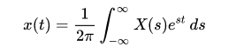
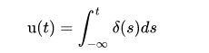


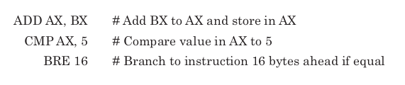
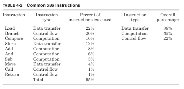

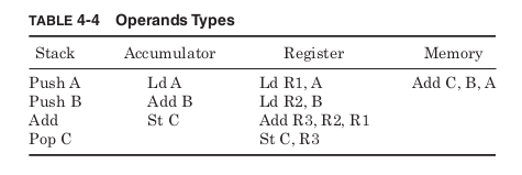

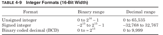

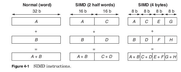
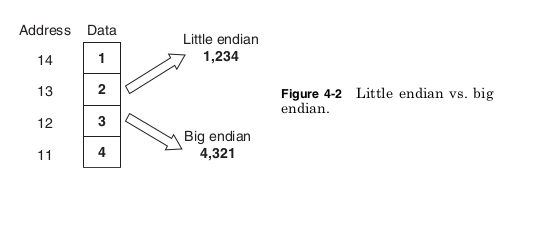


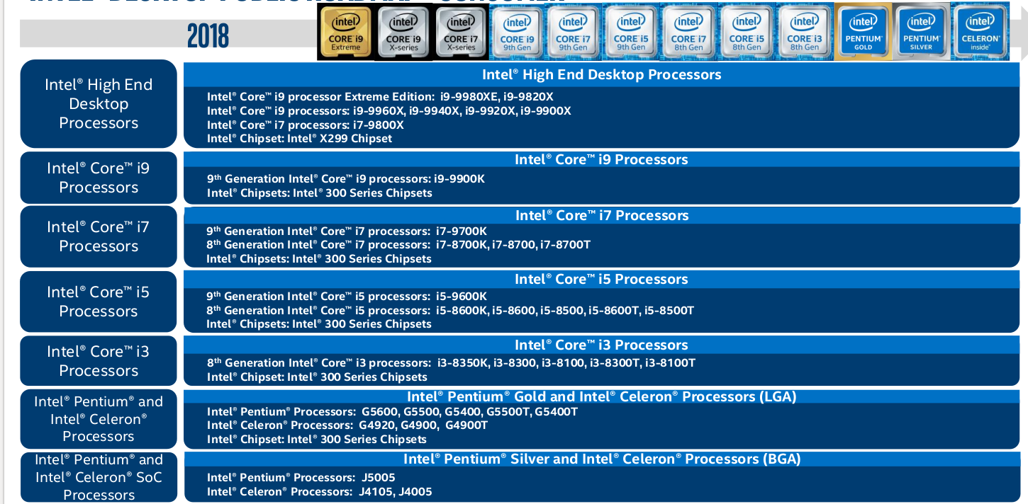

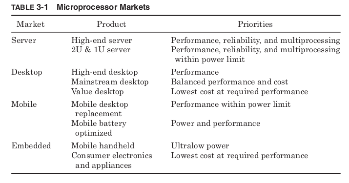


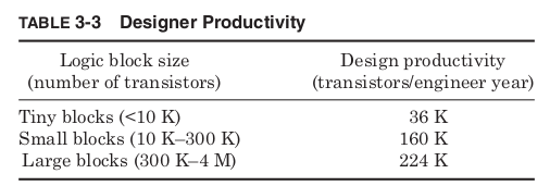
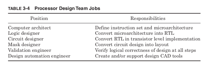
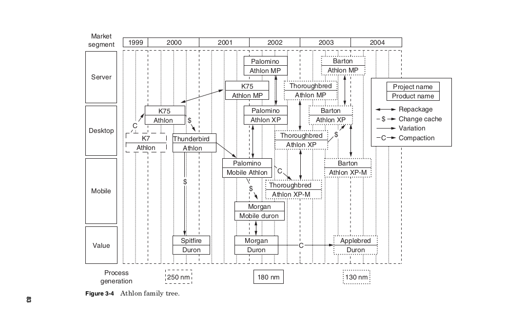
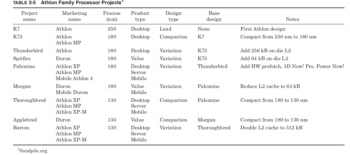
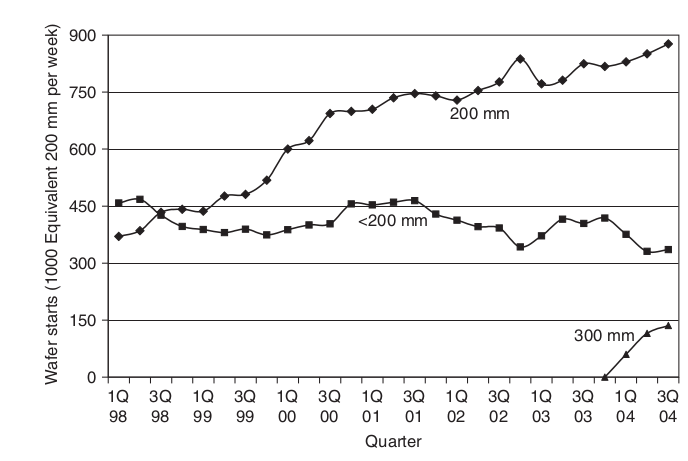


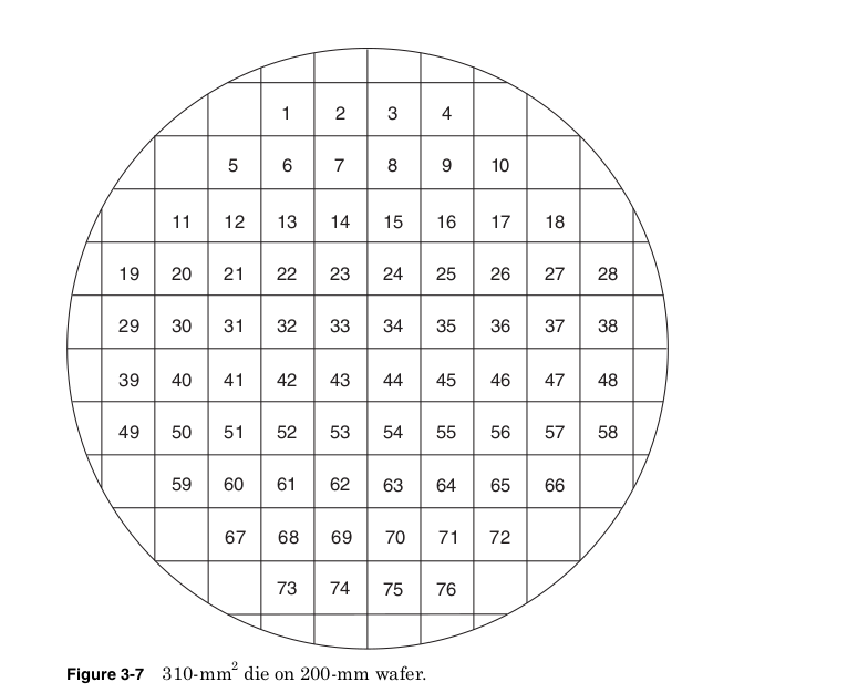
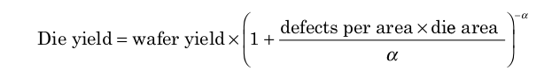
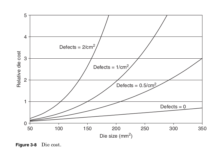


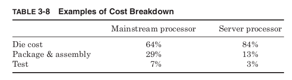

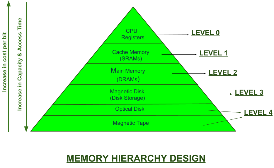
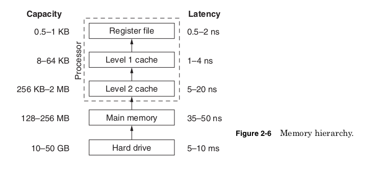


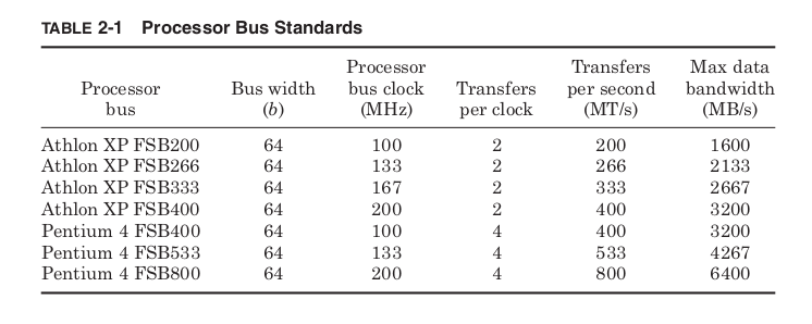
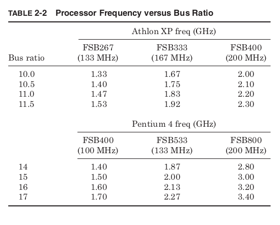


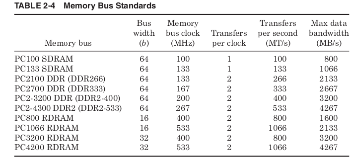


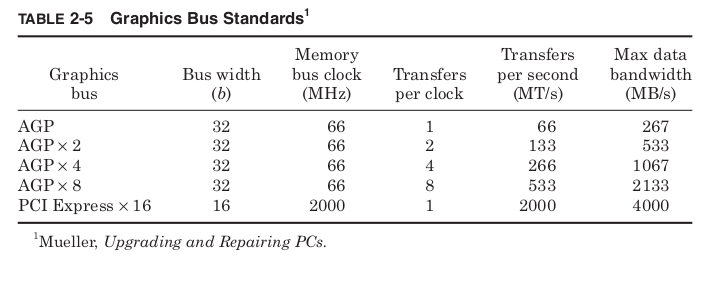


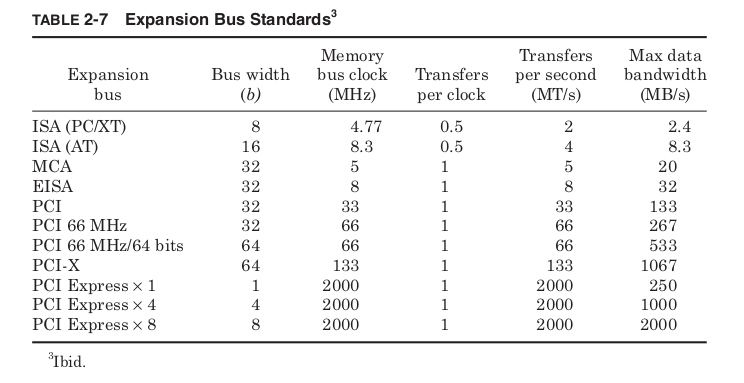


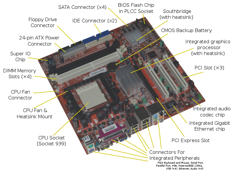
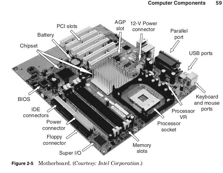


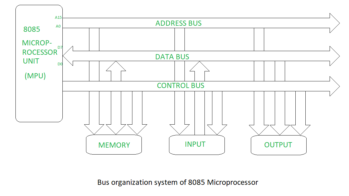


![{\displaystyle I_{\text{D}}={\frac {\mu _{n}C_{\text{ox}}}{2}}{\frac {W}{L}}\left[V_{\text{GS}}-V_{\text{th}}\right]^{2}\left[1+\lambda (V_{\text{DS}}-V_{\text{DSsat}})\right].}](https://wikimedia.org/api/rest_v1/media/math/render/svg/f6593b8932bc4a92e53bfce27d1c29b1254b0ed3)


